SCAS922A February 2012 – April 2016 CDCM9102
PRODUCTION DATA.
- 1 Features
- 2 Applications
- 3 Description
- 4 Revision History
- 5 Device Comparison Table
- 6 Pin Configuration and Functions
- 7 Specifications
- 8 Parameter Measurement Information
- 9 Detailed Description
- 10Application and Implementation
- 11Power Supply Recommendations
- 12Layout
- 13Device and Documentation Support
- 14Mechanical, Packaging, and Orderable Information
Package Options
Mechanical Data (Package|Pins)
- RHB|32
Thermal pad, mechanical data (Package|Pins)
- RHB|32
Orderable Information
9 Detailed Description
9.1 Overview
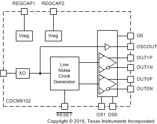
The CDCM9102 is a high-performance PLL that generates 2 copies of commonly-used reference clocks with less than 1-ps RMS jitter from a low-cost crystal.
9.2 Functional Block Diagrams

9.3 Feature Description
The CDCM9102 includes an on-chip PLL with an on-chip VCO. The PLL blocks consist of a crystal input interface, a phase frequency detector (PFD), a charge pump, an on-chip loop filter, and prescaler and feedback dividers. Completing the CDCM9102 device are the output divider and universal output buffer. The PLL and output divider are pre-programmed to generate 2 copies of 100 MHz in LVCMOS, LVPECL or LVDS format.
The PLL is powered by on-chip, low-dropout (LDO) linear voltage regulators. The regulated supply network is partitioned such that the sensitive analog supplies are powered from separate LDOs rather than the digital supplies which use a separate LDO regulator. These LDOs provide isolation for the PLL from any noise in the external power-supply rail. The REG_CAP1 and REG_CAP2 pins should each be connected to ground by 10-μF capacitors to ensure stability.
9.4 Device Functional Modes
9.4.1 Crystal Input (XIN) Interface
The CDCM9102 implements a Colpitts oscillator; therefore, one side of the crystal connects to the XIN pin and the other crystal terminal connects to ground. The device requires the use of a fundamental-mode crystal, and the oscillator operates in parallel resonance mode. The correct load capacitance is necessary to ensure that the circuit oscillates properly. The load capacitance comprises all capacitances in the oscillator feedback loop (the capacitances seen between the terminals of the crystal in the circuit). It is important to account for all sources of capacitance when calculating the correct value for the external discrete load capacitance shown in Figure 8.
 Figure 8. Configuration of Circuit for CDCM9102 XIN Oscillator
The CDCM9102 has been characterized with 10-pF parallel-resonant crystals. The input stage of the crystal oscillator in the CDCM9102 is designed to oscillate at the correct frequency for all parallel-resonant crystals with low-pull capability and rated with a load capacitance that is equal to the sum of the on-chip load capacitance at the XIN pin (CIN = 10 pF maximum), crystal stray capacitance, and board parasitic capacitance between the crystal and XIN pin. To minimize stray and parasitic capacitances, minimize the trace distance routed from the crystal to the XIN pin and avoid other active traces and active circuitry in the area of the crystal oscillator circuit. Table 1 lists crystal types that have been evaluated with the CDCM9102.
Table 1. CDCM9102 Crystal Recommendations
| MANUFACTURER | PART NUMBER |
|---|---|
| Vectron | VXC1-1134 25M0000000 |
| Fox | 218-3 |
| Saronix | FP2500002 |
A mismatch of the load capacitance results in a frequency error according to Equation 1.

where
- Δƒ is the frequency error required by the application.
- f is the fundamental frequency of the crystal.
- CS is the motional capacitance of the crystal. This is a parameter in the data sheet of the crystal.
- C0 is the shunt capacitance of the crystal. This is a parameter in the data sheet of the crystal.
- CLr is the rated load capacitance of the crystal. This is a parameter in the data sheet of the crystal.
- CLa is the actual load capacitance implemented on the PCB (CIN + stray capacitance + parasitic capacitance + CL).
The difference between the rated load capacitance (from the crystal datasheet) and the actual load capacitance (CLa = CIN + CL + CSTRAY + CPARASITIC) should be minimized. A crystal with a low pullability rating (low CS) is ideal.
Design Example:
Desired frequency tolerance Δf ≤ ±80 ppm
Crystal Vendor Parameters:
Intrinsic Frequency Tolerance = ±30 ppm
C0 = 7 pF (shunt capacitance)
CS = 10 fF (motional capacitance)
CLr = 12 pF (load capacitance)
Substituting these parameters into Equation 1 yields a maximum value of CLa = 17 pF to achieve the desired Δf (±50 ppm). Recall that CLa = CIN + CL + CSTRAY + CPARASITIC = 8 pF + (CL + CSTRAY + CPARASITIC). Ideally, the load presented to this crystal should be 12 pF; therefore, the sum of (CL + CSTRAY + CPARASITIC) must be less than 9 pF. Stray and parasitic capacitance must be controlled. This is because the Colpitts oscillator is particularly sensitive to capacitance in parallel with the crystal; therefore, good layout practice is essential. TI recommends that the designer extract the stray and parasitic capacitance from the printed-circuit board design tool and adjust CL accordingly to achieve CLr = CLa. In common scenarios, the external load capacitor is often unnecessary; however, TI recommends that pads be implemented to accommodate an external load capacitor so that the ppm error can be minimized.
9.4.2 Interfacing between LVPECL and HCSL (PCI Express)
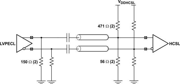
Certain PCI Express applications require HCSL signaling. Because the common-mode voltage for LVPECL and HCSL are different, applications requiring HCSL signaling must use AC-coupling as shown in Figure 9. The
150-Ω resistors ensure proper biasing of the CDCM9102 LVPECL output stage. The 471-Ω and 56-Ω resistor network biases the HCSL receiver input stage.

9.5 Programming
Table 2 and Table 3 list the pin controls and pin configurations of the CDCM9102 output. Table 4 lists the device reset.
9.5.1 Device Configuration
Table 2. CDCM9102 Pin Control of Output Enable
| OE (Pin 7) | MODE | DEVICE CORE | OUTPUT |
|---|---|---|---|
| 0 | Power down | Power down | Hi-Z |
| 1 | Normal | Active | Active |
Table 3. CDCM9102 Pin Configuration of Output Type
| CONTROL PINS | OUTPUT MODE | |
|---|---|---|
| OS1 (Pin 10) | OS0 (Pin 11) | |
| 0 | 0 | LVCMOS, OSCOUT = OFF |
| 0 | 1 | LVDS, OSCOUT = OFF |
| 1 | 0 | LVPECL, OSCOUT = OFF |
| 1 | 1 | LVPECL, OSCOUT = ON |
Table 4. CDCM9102 Device Reset
| RESET (Pin 12) | OPERATING MODE | DEVICE OUTPUTS |
|---|---|---|
| 0 | Device reset | Hi-Z |
| 0 → 1 | Clock generator calibration | Hi-Z |
| 1 | Normal | Active |