SCAS922A February   2012  – April 2016 CDCM9102

PRODUCTION DATA.  

  1. Features
  2. Applications
  3. Description
  4. Revision History
  5. Device Comparison Table
  6. Pin Configuration and Functions
  7. Specifications
    1. 7.1 Absolute Maximum Ratings
    2. 7.2 ESD Ratings
    3. 7.3 Recommended Operating Conditions
    4. 7.4 Thermal Information
    5. 7.5 Electrical Characteristics
    6. 7.6 Timing Requirements
    7. 7.7 Typical Characteristics
  8. Parameter Measurement Information
    1. 8.1 Test Configurations
  9. Detailed Description
    1. 9.1 Overview
    2. 9.2 Functional Block Diagrams
    3. 9.3 Feature Description
    4. 9.4 Device Functional Modes
      1. 9.4.1 Crystal Input (XIN) Interface
      2. 9.4.2 Interfacing between LVPECL and HCSL (PCI Express)
    5. 9.5 Programming
      1. 9.5.1 Device Configuration
  10. 10Application and Implementation
    1. 10.1 Application Information
      1. 10.1.1 Start-Up Time Estimation
      2. 10.1.2 Output Termination
      3. 10.1.3 LVPECL Termination
      4. 10.1.4 LVDS Termination
      5. 10.1.5 LVCMOS Termination
      6. 10.1.6 PCI Express Applications
    2. 10.2 Typical Application
      1. 10.2.1 Design Requirements
      2. 10.2.2 Detailed Design Procedure
        1. 10.2.2.1 Device Selection
          1. 10.2.2.1.1 Calculation Using LCM
        2. 10.2.2.2 Device Configuration
      3. 10.2.3 Application Curve
  11. 11Power Supply Recommendations
    1. 11.1 Thermal Management
    2. 11.2 Power Supply Filtering
  12. 12Layout
    1. 12.1 Layout Guidelines
    2. 12.2 Layout Example
  13. 13Device and Documentation Support
    1. 13.1 Community Resources
    2. 13.2 Trademarks
    3. 13.3 Electrostatic Discharge Caution
    4. 13.4 Glossary
  14. 14Mechanical, Packaging, and Orderable Information

Package Options

Mechanical Data (Package|Pins)
Thermal pad, mechanical data (Package|Pins)
Orderable Information

12 Layout

12.1 Layout Guidelines

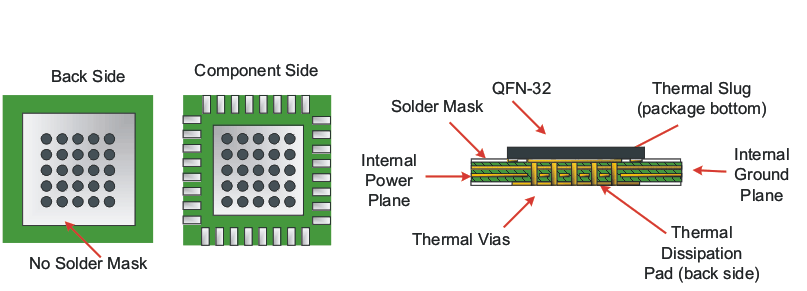
The CDCM9102 is a high-performance device; therefore, pay careful attention to device configuration and printed-circuit board layout with respect to power consumption. Observing good thermal layout practices enables the thermal pad on the backside of the 32-pin VQFN package to provide a good thermal path between the die contained within the package and the ambient air. This thermal pad also serves as the ground connection the device; therefore, a low inductance connection to the ground plane is essential.

12.2 Layout Example

Figure 21 shows a general recommendation of PCB layout with the CDCM9102 that ensures good system-level thermal reliability.
CDCM9102 pcb_lay_cas882.gif Figure 21. Recommended PCB Layout