SLPS601B April 2016 – February 2022 CSD23280F3
PRODUCTION DATA
- 1Features
- 2Applications
- 3Description
- 4Revision History
- 5Specifications
- 6Device and Documentation Support
- 7Mechanical, Packaging, and Orderable Information
Package Options
Refer to the PDF data sheet for device specific package drawings
Mechanical Data (Package|Pins)
- YJM|3
Thermal pad, mechanical data (Package|Pins)
Orderable Information
3 Description
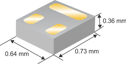
This –12-V, 97-mΩ, P-Channel FemtoFET™ MOSFET is designed and optimized to minimize the footprint in many handheld and mobile applications. This technology is capable of replacing standard small signal MOSFETs while providing a substantial reduction in footprint size.
 Typical Part Dimensions
Product Summary
| TA = 25°C | TYPICAL VALUE | UNIT | ||
|---|---|---|---|---|
| VDS | Drain-to-Source Voltage | –12 | V | |
| Qg | Gate Charge Total (4.5 V) | 0.95 | nC | |
| Qgd | Gate Charge Gate-to-Drain | 0.068 | nC | |
| RDS(on) | Drain-to-Source On-Resistance |
VGS = –1.5 V | 230 | mΩ |
| VGS = –1.8 V | 180 | |||
| VGS = –2.5 V | 129 | |||
| VGS = –4.5 V | 97 | |||
| VGS(th) | Threshold Voltage | –0.65 | V | |
Device Information(1)
| DEVICE | QTY | MEDIA | PACKAGE | SHIP |
|---|---|---|---|---|
| CSD23280F3 | 3000 | 7-Inch Reel | Femto 0.73-mm × 0.64-mm Land Grid Array (LGA) |
Tape and Reel |
| CSD23280F3T | 250 |
(1) For all available packages, see the orderable addendum at the
end of the data sheet.
Absolute Maximum Ratings
| TA = 25°C | VALUE | UNIT | |
|---|---|---|---|
| VDS | Drain-to-Source Voltage | –12 | V |
| VGS | Gate-to-Source Voltage | –6 | V |
| ID | Continuous Drain Current(1) | 2.9 | A |
| Continuous Drain Current(2) | 1.8 | ||
| IDM | Pulsed Drain Current(1)(3) | 11.4 | A |
| PD | Power Dissipation(1) | 1.4 | W |
| Power Dissipation(2) | 0.5 | ||
| V(ESD) | Human-Body Model (HBM) | 4000 | V |
| Charged-Device Model (CDM) | 2000 | ||
| TJ, Tstg |
Operating Junction, Storage Temperature |
–55 to 150 | °C |
(1) Typical RθJA = 90°C/W on 1-in2
(6.45-cm2), 2-oz (0.071-mm) thick Cu pad on a 0.06-in (1.52-mm)
thick FR4 PCB
(2) Typical RθJA = 255°C/W on min Cu board
(3) Pulse duration ≤ 100 μs, duty cycle ≤ 1%.
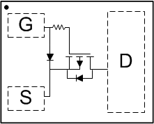
 Top View