SLPS418A June 2013 – June 2014 CSD75207W15
PRODUCTION DATA.
- 1Features
- 2Applications
- 3Description
- 4Revision History
- 5Specifications
- 6Device and Documentation Support
- 7Mechanical, Packaging, and Orderable Information
Package Options
Refer to the PDF data sheet for device specific package drawings
Mechanical Data (Package|Pins)
- YZF|9
Thermal pad, mechanical data (Package|Pins)
Orderable Information
7 Mechanical, Packaging, and Orderable Information
The following pages include mechanical packaging and orderable information. This information is the most current data available for the designated devices. This data is subject to change without notice and revision of this document. For browser-based versions of this data sheet, refer to the left-hand navigation.
7.1 CSD75207W15 Package Dimensions
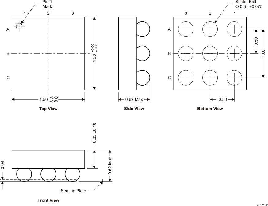
NOTE:
All dimensions are in mm (unless otherwise specified)Pinout
| POSITION | DESIGNATION |
|---|---|
| A1 | Gate1 |
| A2, A3, B3 | Drain1 |
| C1 | Gate2 |
| C2, C3, B2 | Drain2 |
| B1 | Source Sense |
7.2 Recommended PCB Land Pattern
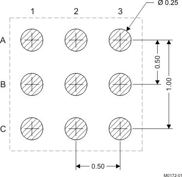
NOTE:
All dimensions are in mm (unless otherwise specified).7.3 Tape and Reel Information
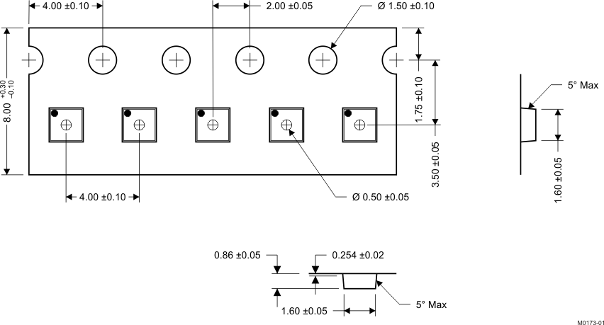
NOTE:
All dimensions are in mm (unless otherwise specified).