SLPS418A June 2013 – June 2014 CSD75207W15
PRODUCTION DATA.
- 1Features
- 2Applications
- 3Description
- 4Revision History
- 5Specifications
- 6Device and Documentation Support
- 7Mechanical, Packaging, and Orderable Information
Package Options
Refer to the PDF data sheet for device specific package drawings
Mechanical Data (Package|Pins)
- YZF|9
Thermal pad, mechanical data (Package|Pins)
Orderable Information
5 Specifications
5.1 Electrical Characteristics
(TA = 25°C unless otherwise stated). Specifications and graphs are Per MOSFET unless otherwise stated. Drain to Drain measurements are done with both MOSFETs in series (common source configuration.| PARAMETER | TEST CONDITIONS | MIN | TYP | MAX | UNIT | ||
|---|---|---|---|---|---|---|---|
| STATIC CHARACTERISTICS | |||||||
| BVD1D2 | Drain-to-Drain Voltage | VGS = 0 V, ID1D2 = –250 μA | –20 | V | |||
| BVGSS | Gate-to-Source Voltage | VD1D2 = 0 V, IG = -250 μA | –6 | V | |||
| IDDS | Drain-to-Drain Leakage Current | VGS = 0 V, VD1D2 = –16 V | –1 | μA | |||
| IGSS | Gate-to-Source Leakage Current | VD1D2 = 0 V, VGS = –6 V | –100 | nA | |||
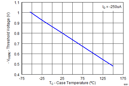
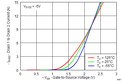
| VGS(th) | Gate-to-Source Threshold Voltage | VD1D2 = VGS, IDS = –250 μA | –0.6 | –0.8 | –1.1 | V | |
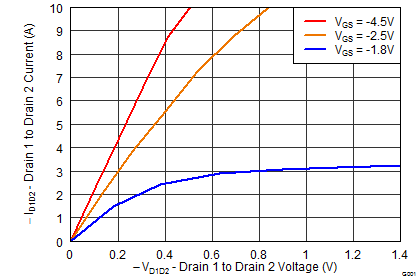
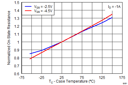
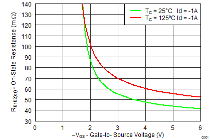
| RD1D2(on) | Drain-to-Drain On-Resistance | VGS = –1.8 V, ID1D2 = –1 A | 119 | 162 | mΩ | ||
| VGS = –2.5 V, ID1D2 = –1 A | 64 | 77 | mΩ | ||||
| VGS = –4.5 V, ID1D2 = –1 A | 45 | 54 | mΩ | ||||
| gfs | Transconductance | VD1D2 = –10 V, ID1D2 = –1 A | 6.2 | S | |||
| DYNAMIC CHARACTERISTICS | |||||||
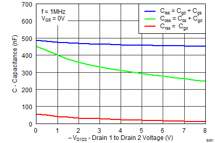
| CISS | Input Capacitance | VGS = 0 V, VD1D2 = –10 V, ƒ = 1 MHz |
458 | 595 | pF | ||
| COSS | Output Capacitance | 225 | 293 | pF | |||
| CRSS | Reverse Transfer Capacitance | 10.4 | 13.5 | pF | |||
| Rg | Series Gate Resistance | 27 | Ω | ||||
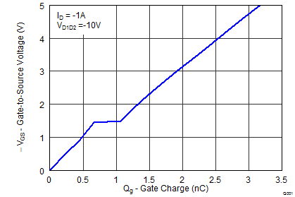
| Qg | Gate Charge Total (–4.5 V) | VD1D2 = –10 V, ID1D2 = –1 A |
2.9 | 3.7 | nC | ||
| Qgd | Gate Charge – Gate to Drain | 0.4 | nC | ||||
| Qgs | Gate Charge – Gate to Source | 0.7 | nC | ||||
| Qg(th) | Gate Charge at Vth | 0.4 | nC | ||||
| QOSS | Output Charge | VD1D2 = –9.5 V, VGS = 0 V | 3.1 | nC | |||
| td(on) | Turn On Delay Time | VD1D2 = –10 V, VGS = –4.5 V, ID1D2 = –1 A, RG = 30 Ω |
12.8 | ns | |||
| tr | Rise Time | 8.6 | ns | ||||
| td(off) | Turn Off Delay Time | 32.1 | ns | ||||
| tf | Fall Time | 16.0 | ns | ||||
| DIODE CHARACTERISTICS | |||||||
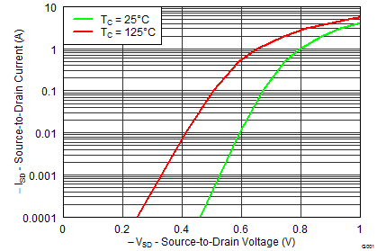
| VSD | Diode Forward Voltage | ID1D2 = –1 A, VGS = 0 V | –0.8 | –1 | V | ||
| Qrr | Reverse Recovery Charge | Vdd = –10 V, IF = –1 A, di/dt = 200 A/μs | 10.5 | nC | |||
| trr | Reverse Recovery Time | Vdd = –10 V, IF = –1 A, di/dt = 200 A/μs | 23 | ns | |||
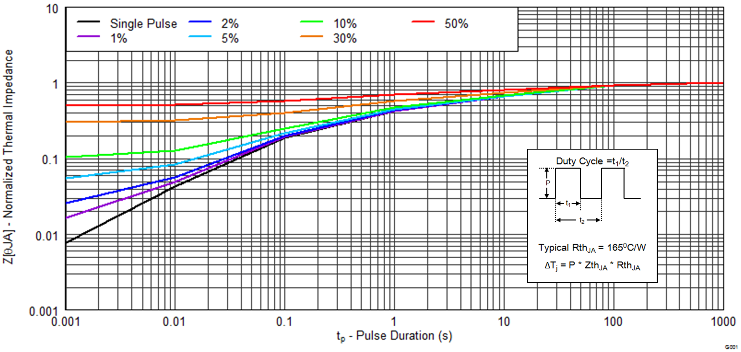
5.2 Thermal Information
(TA = 25°C unless otherwise stated)| THERMAL METRIC | TYPICAL VALUE | UNIT | |||
|---|---|---|---|---|---|
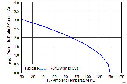
| R θJA | Junction-to-Ambient Thermal Resistance(1)(3) | 70 | °C/W | ||
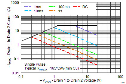
| Junction-to-Ambient Thermal Resistance (2)(3) | 165 | ||||
(1) Device mounted on FR4 material with Minimum Cu mounting area.
(2) Device mounted on FR4 material with 1-inch2 of Cu (2 oz).
(3) Measured with both devices biased in a parallel condition.
 |
Typ RθJA = 70°C/W when mounted on 1-inch2 of 2 oz. Cu. |
 |
Typ RθJA = 165°C/W when mounted on minimum pad area of 2-oz. Cu. |
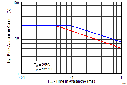
5.3 Typical MOSFET Characteristics
(TA = 25°C unless otherwise stated)