SLPS458A December 2013 – August 2014 CSD95373AQ5M
PRODUCTION DATA.
- 1 Features
- 2 Applications
- 3 Description
- 4 Revision History
- 5 Pin Configuration And Functions
- 6 Specifications
- 7 Detailed Description
- 8 Application and Implementation
- 9 Layout
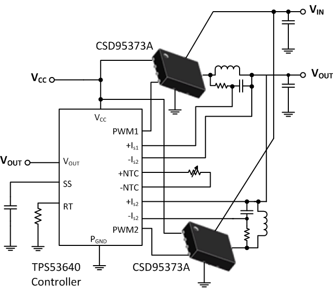
- 10Application Schematic
- 11Device and Documentation Support
- 12Mechanical, Packaging, and Orderable Information
Package Options
Mechanical Data (Package|Pins)
- DQP|12
Thermal pad, mechanical data (Package|Pins)
Orderable Information
1 Features
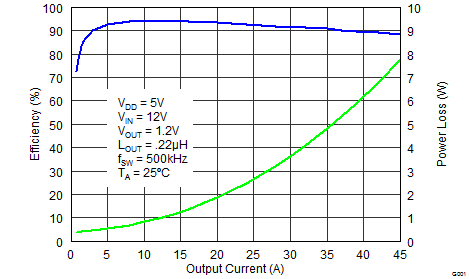
- 45 A Continuous Operating Current Capability
- 92.6% System Efficiency at 25 A
- Ultra-Low Power Loss of 2.6 W at 25 A
- High Frequency Operation (up to 2 MHz)
- High Density – SON 5 × 6-mm Footprint
- Ultra-Low Inductance Package
- System Optimized PCB Footprint
- 3.3 V and 5 V PWM Signal Compatible
- Diode Emulation Mode with FCCM
- Analog Temperature Output
- Tri-State PWM Input
- Integrated Bootstrap Switch
- Optimized Dead Time for Shoot Through Protection
- RoHS Compliant – Lead-Free Terminal Plating
- Halogen Free
2 Applications
- Multiphase Synchronous Buck Converter
- High Frequency Applications
- High-Current, Low Duty Cycle Applications
- Point of Load Dc-Dc Converters
- Memory and Graphic Cards
- Desktop and Server VR11.× and VR12.× for VCore Synchronous Buck Converters
3 Description
The CSD95373AQ5M NexFET™ Power Stage is a highly-optimized design for use in a high-power, high-density Synchronous Buck converters. This product integrates the driver IC and NexFET technology to complete the power stage switching function. The driver IC has a built-in selectable diode emulation function that enables DCM operation to improve light load efficiency. This combination produces high current, high efficiency, and high speed switching capability in a small 5 × 6 mm outline package. It also integrates the temperature sensing functionality to simplify system design and improve accuracy. In addition, the PCB footprint has been optimized to help reduce design time and simplify the completion of the overall system design.
Device Information(1)
| Device | Media | Qty | Package | Ship |
|---|---|---|---|---|
| CSD95373AQ5M | 13-Inch Reel | 2500 | SON 5-mm × 6-mm Package |
Tape and Reel |
| CSD95373AQ5MT | 7-Inch Reel | 250 |
- For all available packages, see the orderable addendum at the end of the data sheet.
Application Diagram
Typical Power Stage Efficiency and Power Loss