SLPS458A December 2013 – August 2014 CSD95373AQ5M
PRODUCTION DATA.
- 1 Features
- 2 Applications
- 3 Description
- 4 Revision History
- 5 Pin Configuration And Functions
- 6 Specifications
- 7 Detailed Description
- 8 Application and Implementation
- 9 Layout
- 10Application Schematic
- 11Device and Documentation Support
- 12Mechanical, Packaging, and Orderable Information
Package Options
Mechanical Data (Package|Pins)
- DQP|12
Thermal pad, mechanical data (Package|Pins)
Orderable Information
12 Mechanical, Packaging, and Orderable Information
The following pages include mechanical, packaging, and orderable information. This information is the most current data available for the designated devices. This data is subject to change without notice and revision of this document. For browser-based versions of this data sheet, refer to the left-hand navigation.
12.1 Mechanical Drawing
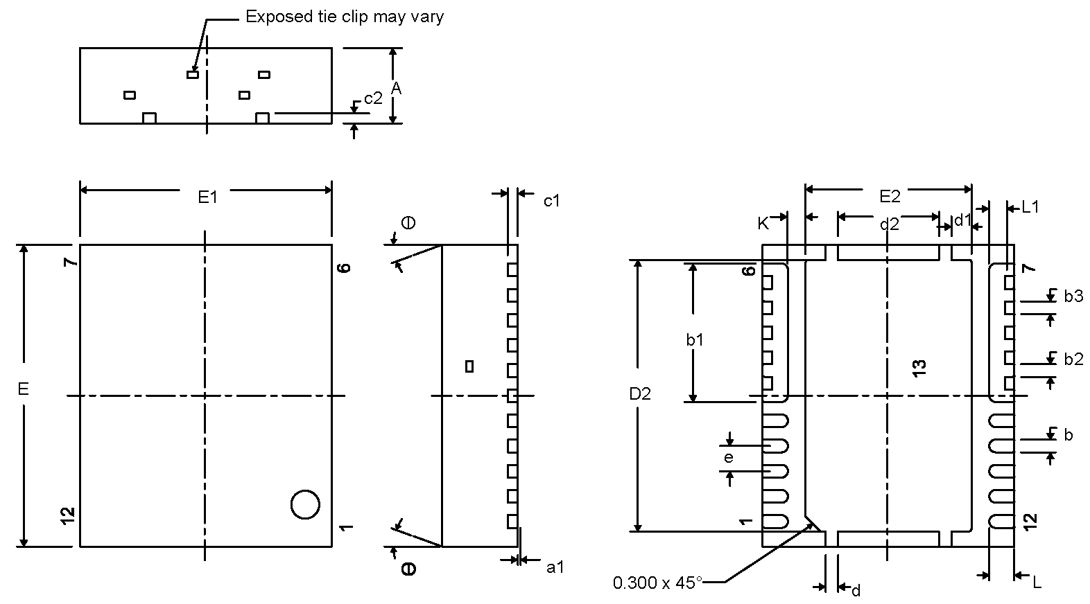
| DIM | MILLIMETERS | INCHES | ||||
|---|---|---|---|---|---|---|
| MIN | NOM | MAX | MIN | NOM | MAX | |
| A | 1.400 | 1.450 | 1.500 | 0.055 | 0.057 | 0.059 |
| a1 | 0.000 | 0.000 | 0.050 | 0.000 | 0.000 | 0.002 |
| b | 0.200 | 0.250 | 0.320 | 0.008 | 0.010 | 0.013 |
| b1 | 2.750 TYP | 0.108 TYP | ||||
| b2 | 0.200 | 0.250 | 0.320 | 0.008 | 0.010 | 0.013 |
| b3 | 0.250 TYP | 0.010 TYP | ||||
| c1 | 0.150 | 0.200 | 0.250 | 0.006 | 0.008 | 0.010 |
| D2 | 5.300 | 5.400 | 5.500 | 0.209 | 0.213 | 0.217 |
| d | 0.200 | 0.250 | 0.300 | 0.008 | 0.010 | 0.012 |
| d1 | 0.350 | 0.400 | 0.450 | 0.014 | 0.016 | 0.018 |
| d2 | 1.900 | 2.000 | 2.100 | 0.075 | 0.079 | 0.083 |
| E | 5.900 | 6.000 | 6.100 | 0.232 | 0.236 | 0.240 |
| E1 | 4.900 | 5.000 | 5.100 | 0.193 | 0.197 | 0.201 |
| E2 | 3.200 | 3.300 | 3.400 | 0.126 | 0.130 | 0.134 |
| e | 0.500 TYP | 0.020 TYP | ||||
| K | 0.350 TYP | 0.014 TYP | ||||
| L | 0.400 | 0.500 | 0.600 | 0.016 | 0.020 | 0.024 |
| L1 | 0.210 | 0.310 | 0.410 | 0.008 | 0.012 | 0.016 |
| θ | 0.00 | — | — | 0.00 | — | — |
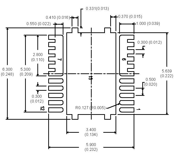
12.2 Recommended PCB Land Pattern
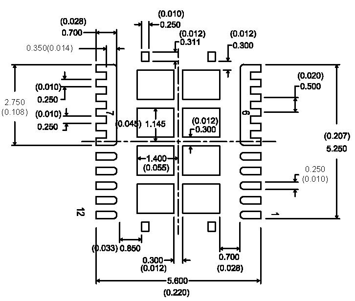
12.3 Recommended Stencil Opening
Notes:
- Dimensions are shown in mm (inches) format
- Stencil thickness is 100 µm.