SLPS458A December 2013 – August 2014 CSD95373AQ5M
PRODUCTION DATA.
- 1 Features
- 2 Applications
- 3 Description
- 4 Revision History
- 5 Pin Configuration And Functions
- 6 Specifications
- 7 Detailed Description
- 8 Application and Implementation
- 9 Layout
- 10Application Schematic
- 11Device and Documentation Support
- 12Mechanical, Packaging, and Orderable Information
Package Options
Mechanical Data (Package|Pins)
- DQP|12
Thermal pad, mechanical data (Package|Pins)
Orderable Information
6 Specifications
6.1 Absolute Maximum Ratings(1)
TA = 25°C (unless otherwise noted)| VALUE | UNIT | |||
|---|---|---|---|---|
| MIN | MAX | |||
| VIN to PGND | –0.3 | 25 | V | |
| VIN to VSW | –0.3 | 25 | V | |
| VIN to VSW (<10 ns) | –7 | 27 | V | |
| VSW to PGND | –0.3 | 20 | V | |
| VSW to PGND (<10 ns) | –7 | 23 | V | |
| VDD to PGND | –0.3 | 7 | V | |
| ENABLE, PWM, FCCM, TAO to PGND(2) | –0.3 | VDD + 0.3 | V | |
| BOOT to BOOT_R(2) | –0.3 | VDD + 0.3 | V | |
| Power Dissipation, PD | 12 | W | ||
| Operating Temperature Range, TJ | –55 | 150 | °C | |
(1) Stresses above those listed in "Absolute Maximum Ratings" may cause permanent damage to the device. These are stress ratings only and functional operation of the device at these or any other conditions beyond those indicated under "Recommended Operating Conditions" is not implied. Exposure to Absolute Maximum rated conditions for extended periods may affect device reliability.
(2) Should not exceed 7 V.
6.2 Handling Ratings
| MIN | MAX | UNIT | |||
|---|---|---|---|---|---|
| Tstg | Storage Temperature Range | –55 | 150 | °C | |
| V(ESD) | Electrostatic discharge | Human Body Model (HBM) | –2000 | 2000 | V |
| Charged Device Model (CDM) | –500 | 500 | |||
6.3 Recommended Operating Conditions
TA = 25° (unless otherwise noted)| MIN | MAX | UNIT | ||
|---|---|---|---|---|
| Gate Drive Voltage, VDD | 4.5 | 5.5 | V | |
| Input Supply Voltage, VIN(1) | 16 | V | ||
| Output Voltage, VOUT | 5.5 | V | ||
| Continuous Output Current, IOUT | VIN = 12 V, VDD = 5 V, VOUT = 1.8 V, ƒSW = 500 kHz, LOUT = 0.22 µH(2) |
45 | A | |
| Peak Output Current, IOUT-PK(3) | 67 | A | ||
| Switching Frequency, ƒSW | CBST = 0.1 µF (min) | 2000 | kHz | |
| On Time Duty Cycle | ƒSW = 1 MHz | 85% | ||
| Minimum PWM On Time | 20 | ns | ||
| Operating Temperature | –40 | 125 | °C | |
(1) Operating at high VIN can create excessive AC voltage overshoots on the switch node (VSW) during MOSFET switching transients. For reliable operation, the switch node (VSW) to ground voltage must remain at or below the Absolute Maximum Ratings.
(2) Measurement made with six 10-µF (TDK C3216X5R1C106KT or equivalent) ceramic capacitors placed across VIN to PGND pins.
(3) System conditions as defined in Note 1. Peak Output Current is applied for tp = 50 µs.
6.4 Thermal Information
TA = 25°C (unless otherwise noted)| THERMAL METRIC | MIN | TYP | MAX | UNIT | |
|---|---|---|---|---|---|
| RθJC | Junction-to-Case Thermal Resistance (Top of package)(1) | 15 | °C/W | ||
| RθJB | Junction-to-Board Thermal Resistance(2) | 2 | |||
(1) RθJC is determined with the device mounted on a 1-inch² (6.45-cm²), 2-oz (.071-mm thick) Cu pad on a 1.5-inches x 1.5-inches,
0.06-inch (1.52-mm) thick FR4 board.
0.06-inch (1.52-mm) thick FR4 board.
(2) RθJB value based on hottest board temperature within 1 mm of the package.
6.5 Electrical Characteristics
TA = 25°C, VDD = POR to 5.5 V (unless otherwise noted)| PARAMETER | CONDITIONS | MIN | TYP | MAX | UNIT |
|---|---|---|---|---|---|
| PLOSS | |||||
| Power Loss(1) | VIN = 12 V, VDD = 5 V, VOUT = 1.2 V, IOUT = 25 A, ƒSW = 500 kHz, LOUT = 0.22 µH , TJ = 25°C |
2.6 | W | ||
| Power Loss(2) | VIN = 12 V, VDD = 5 V, VOUT = 1.2 V, IOUT = 25 A, ƒSW = 500 kHz, LOUT = 0.22 µH , TJ = 125°C |
3.3 | W | ||
| VIN | |||||
| VIN Quiescent Current, IQ | ENABLE = 0, VDD = 5 V | 10 | µA | ||
| VDD | |||||
| Standby Supply Current, IDD | ENABLE = 0, PWM = 0 | 250 | µA | ||
| Operating Supply Current, IDD | ENABLE = 5 V, PWM = 50% Duty cycle, ƒSW = 500 kHz |
16 | mA | ||
| POWER-ON RESET AND UNDER VOLTAGE LOCKOUT | |||||
| Power-On Reset, VDD Rising | 3.6 | 3.9 | V | ||
| UVLO, VDD Falling | 3.4 | 3.7 | V | ||
| Hysteresis | 100 | 250 | mV | ||
| Startup Delay(3) | ENABLE = 5 V | 6 | µs | ||
| ENABLE | |||||
| Logic Level High, VIH | Schmitt Trigger Input See Figure 12 |
2 | V | ||
| Logic Level Low, VIL | 0.8 | V | |||
| Weak Pulldown Impedance | 100 | kΩ | |||
| Rising Propagation Delay, tPDH | 3 | µs | |||
| Falling Propagation Delay, tPDL | 30 | ns | |||
| FCCM(2) | |||||
| Logic Level High, VIH | Schmitt Trigger Input See Figure 14 and Figure 15 |
2 | V | ||
| Logic Level Low, VIL | 0.8 | V | |||
| Weak Pullup Current | 5 | µA | |||
| THERMAL SHUTDOWN(2) | |||||
| Start Threshold | 150 | 165 | °C | ||
| Temperature Hysteresis | 25 | °C | |||
| PWM | |||||
| IPWMH | PWM = 5 V | 500 | µA | ||
| IPWML | PWM = 0 | –500 | µA | ||
| PWM Logic Level High, VPWMH | CPWM = 10 pF | 2.3 | 2.5 | 2.7 | V |
| PWM Logic Level Low, VPWML | 0.7 | 0.9 | 1.1 | V | |
| PWM Tri-State Open Voltage | 1.5 | V | |||
| PWM to VSW Propagation Delay, tPDLH and tPDHL(2) | 50 | ns | |||
| Tri-State Shutdown Hold-off Time, t3HT(2) | 30 | ns | |||
| Tri-State Shutdown Propagation Delay, t3SD(2) | 80 | 160 | ns | ||
| Tri-State Recovery Propagation Delay, t3RD(2) | 50 | 80 | ns | ||
| Diode Emulation Minimum On Time, tDEM(2) | 150 | ns | |||
| BOOTSTRAP SWITCH | |||||
| Forward Voltage, VFBOOT | Measured from VDD to VBOOT, IF = 10 mA | 200 | 360 | mV | |
| Reverse Leakage, IRBOOT(1) | VBOOT – VDD = 20 V | 0.15 | 1 | µA | |
| ZERO CROSSING COMPARATOR | |||||
| LS FET Turn-off Current | Diode Emulation Mode Enabled VOUT = 1.8 V, L = 150 nH |
0 | 1.1 | A | |
| THERMAL ANALOG OUTPUT TAO | |||||
| Output Voltage at 25°C | 0.56 | 0.60 | 0.64 | V | |
| Output Voltage Temperature Coefficient | 8 | mV/°C | |||
(1) Measurement made with six 10-µF (TDK C3216X5R1C106KT or equivalent) ceramic capacitors placed across VIN to PGND pins
(2) Specified by design
(3) POR to VSW Rising
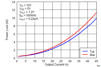
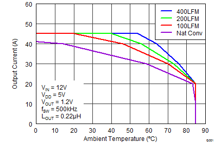
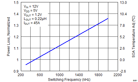
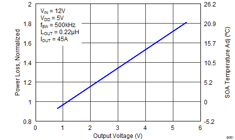
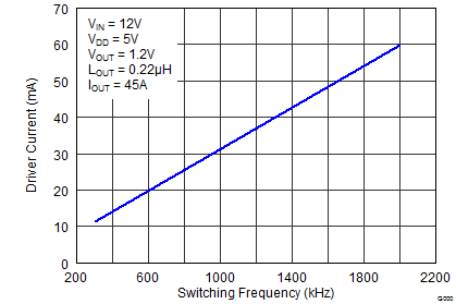
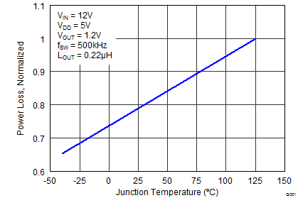
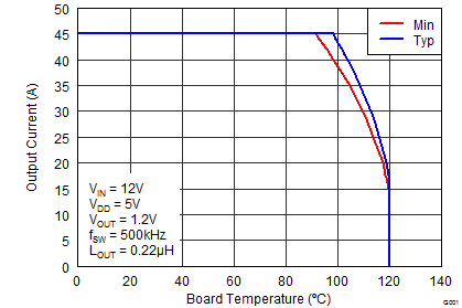
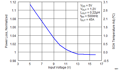
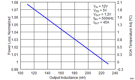
6.6 Typical Power Stage Device Characteristics
TJ = 125°C, unless stated otherwise. The Typical CSD95373A System Characteristic curves are based on measurements made on a PCB design with dimensions of 4-inches (W) × 3.5-inches (L) × 0.062-inch (T) and 6 copper layers of 1-oz. copper thickness. See the Application and Implementation section for detailed explanation.