SLPS458A December 2013 – August 2014 CSD95373AQ5M
PRODUCTION DATA.
- 1 Features
- 2 Applications
- 3 Description
- 4 Revision History
- 5 Pin Configuration And Functions
- 6 Specifications
- 7 Detailed Description
- 8 Application and Implementation
- 9 Layout
- 10Application Schematic
- 11Device and Documentation Support
- 12Mechanical, Packaging, and Orderable Information
Package Options
Mechanical Data (Package|Pins)
- DQP|12
Thermal pad, mechanical data (Package|Pins)
Orderable Information
7 Detailed Description
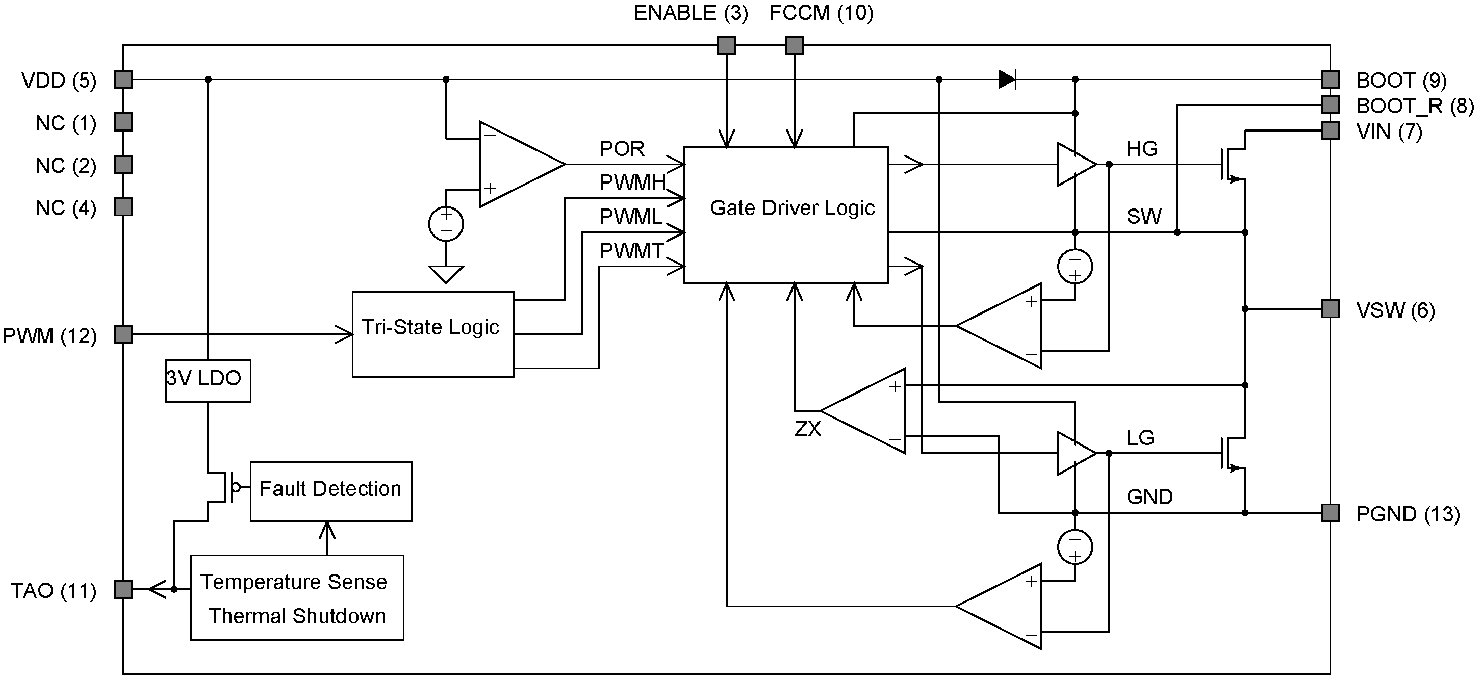
7.1 Functional Block Diagram
7.2 Feature Description
7.2.1 Powering CSD95373AQ5M And Gate Drivers
An external VDD voltage is required to supply the integrated gate driver IC and provide the necessary gate drive power for the MOSFETs. The gate driver IC is capable of supplying in excess of 4 A peak current into the MOSFET gates to achieve fast switching. A 1 µF 10 V X5R or higher ceramic capacitor is recommended to bypass VDD pin to PGND. A bootstrap circuit to provide gate drive power for the Control FET is also included. The bootstrap supply to drive the Control FET is generated by connecting a 100 nF 16 V X5R ceramic capacitor between BOOT and BOOT_R pins. An optional RBOOT resistor can be used to slow down the turn on speed of the Control FET and reduce voltage spikes on the VSW node. A typical 1 to 4.7 Ω value is a compromise between switching loss and VSW spike amplitude.
7.2.2 Undervoltage Lockout Protection (UVLO)
The VDD supply is monitored for UVLO conditions and both Control FET and Sync FET gates are held low until adequate supply is available. An internal comparator evaluates the VDD voltage level and if VDD is greater than the Power On Reset threshold (VPOR), the gate driver becomes active. If VDD is less than the UVLO threshold, the gate driver is disabled and the internal MOSFET gates are actively driven low. At the rising edge of the VDD voltage, both Control FET and Sync FET gates are actively held low during VDD transitions between 1 V to VPOR. This region is referred to as the Gate Drive Latch Zone (see Figure 11). In addition, at the falling edge of the VDD voltage, both Control FET and Sync FET gates are actively held low during the UVLO to 1 V transition.
The Power Stage CSD95373AQ5M device must be powered up and enabled before the PWM signal is applied.
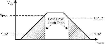 Figure 11. UVLO Operation
7.2.3 Enable
The ENABLE pin is TTL compatible. The logic level thresholds are sustained under all VDD operating conditions between VPOR to VDD. In addition, if this pin is left floating, a weak internal pulldown resistor of 100 kΩ pulls the ENABLE pin below the logic level low threshold. The operational functions of this pin should follow the timing diagram outlined in Figure 12. A logic level low actively holds both Control FET and Sync FET gates low and VDD pin should typically draw less than 5 µA.
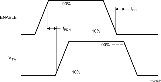 Figure 12. CSD95373AQ5M ENABLE Timing Diagram (VDD = PWM = 5 V)
7.2.4 Power-Up Sequencing
If the ENABLE signal is used, it is necessary to ensure proper co-ordination with the ENABLE and soft-start features of the external PWM controller in the system. If the CSD95373AQ5M was disabled through ENABLE without sequencing with the PWM IC controller, the buck converter output will have no voltage or fall below regulation set point voltage. As a result, the PWM controller IC delivers Max duty cycle on the PWM line. If the Power Stage is re-enabled by driving the ENABLE pin high, there will be an extremely large input inrush current when the output voltage builds back up again. The input inrush current might have undesirable consequences such as inductor saturation, driving the input power supply into current limit or even catastrophic failure of the CSD95373AQ5M device. Disabling the PWM controller is recommended when the CSD95373AQ5M is disabled. The PWM controller should always be re-enabled by going through soft-start routine to control and minimize the input inrush current and reduce current and voltage stress on all buck converter components. TI recommends that the external PWM controller be disabled when CSD95373AQ5M is disabled or nonoperational because of UVLO.
When ENABLE signal is toggled, there is an internal 3 µs hold-off time before the driver responds to PWM events to ensure the analog sensing circuitry is properly powered and stable. This hold-off time should be considered when designing the power-up sequencing of the controller IC and the Power Stage.
7.2.5 PWM
The input PWM pin incorporates a tri-state function. The Control FET and Sync FET gates are forced low if the PWM pin is left floating for more than the tri-state Hold off time (t3HT). The tri-state mode can be entered by actively driving the PWM input to the V3T voltage, or the PWM input can be made high impedance and internal current sources drive PWM to V3T. The PWM input can source up to IPWMH and sink down to IPWML current to drive PWM to the V3T voltage, but consumes no current when sitting at the V3T voltage. Operation in and out of tri-state mode should follow the timing diagram outlined in Figure 13. Both VPWML and VPWMH threshold levels are set to accommodate both 3.3 V and 5 V logic controllers. During typical operation, the PWM signal should be driven to logic levels Low and High with a maximum of 500 Ω sink/source impedance respectively.
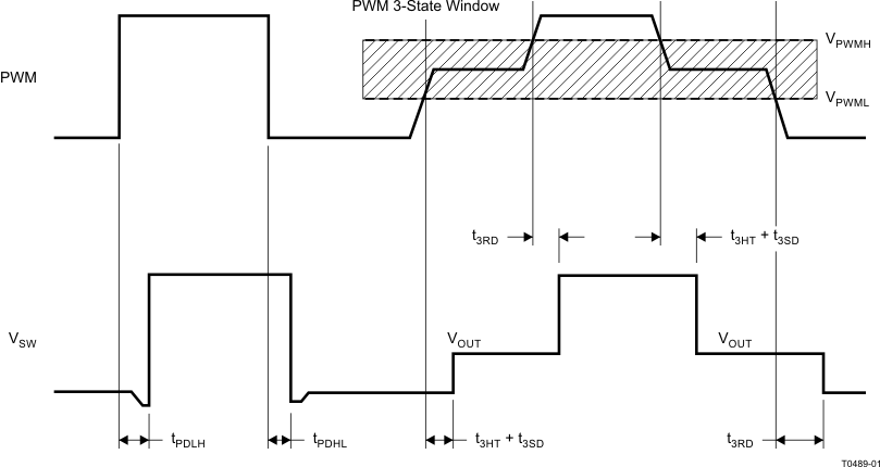 Figure 13. PWM Timing Diagram
7.2.6 FCCM
The input FCCM pin enables the Power Stage device to operate in either continuous current conduction mode or diode emulation mode. When FCCM is driven above its high threshold, the Power Stage operates in continuous conduction mode regardless of the polarity of the output inductor current. When FCCM is driven below its low threshold, the Power Stage's internal zero-cross detection circuit is enabled. When the zero-cross detection circuit is active, diode emulation mode is entered on the third consecutive PWM pulse in which a zero-crossing event is detected. If FCCM is driven high after diode emulation mode has been enabled, continuous conduction mode begins after the next PWM event. See Figure 14 and Figure 15 for FCCM timing
7.2.7 TAO/Fault (Thermal Analog Output/Protection Flag)
During typical operation, the output TAO pin is a highly accurate analog temperature measurement of the lead-frame temperature of the Power Stage. Because the source junction of the Sync FET sits directly on the lead-frame of the Power Stage, this output can be used as an accurate measurement of the junction temperature of the Sync FET. The TAO pin should be bypassed to PGND using a 1 nF X7R ceramic capacitor to ensure accurate temperature measurement.
This Power Stage device has built-in overtemperature protection (described in Overtemperature), which is flagged by pulling TAO to 3.3 V. The TAO pin also includes a built in ORing function. When connecting TAO pins of more than one device together, the TAO bus automatically reads the highest TAO voltage among all devices. This greatly simplifies the temperature sense and fault reporting design for multi-phase applications, where a single line TAO/FAULT bus can be used to tie the TAO pins of all phases together and the system can monitor the temperature of the hottest component.
7.2.7.1 Overtemperature
An overtemperature fault occurs when the dies temperature reaches Thermal Shutdown Temperature (see the Electrical Characteristics). An overtemperature event is the only fault condition to which the Power Stage automatically reacts. When the overtemperature event is detected, the Power Stage automatically turns off both HS and LS MOSFETs and pulls TAO to 3.3 V. If the temperature falls below the overtemperature threshold hysteresis band, the driver again responds to PWM commands and the TAO pin returns to typical operation. A weak pulldown is used to pull TAO back from a fault event, so there is a significant delay before the TAO output reports the correct temperature.
7.2.7.2 Gate Drivers
This Power Stage has an internal high-performance gate driver IC that is trimmed to achieve minimum dead-time for lowest possible switching loss and switch-node ringing reduction. To eliminate the possibility of shoot-through at light load conditions, the dead-time is adjusted to a longer period when the inductor current is negative prior to a PWM HIGH input.
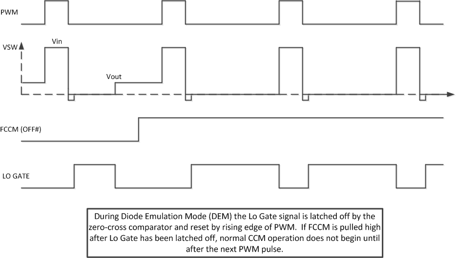 Figure 14. FCCM Rising Timing Diagram
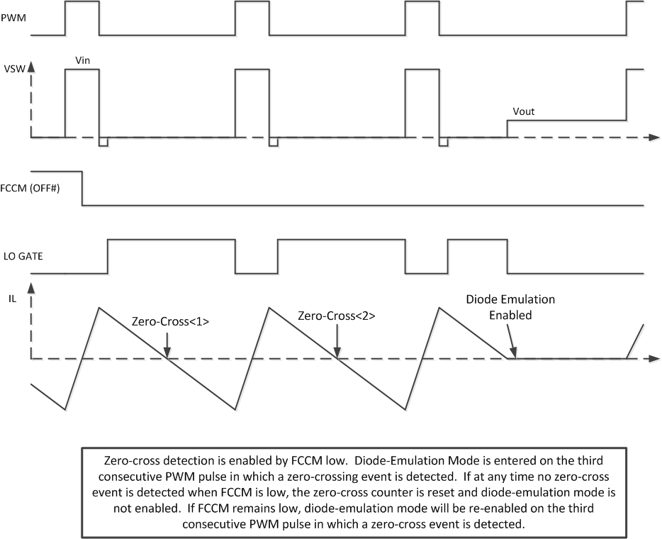 Figure 15. FCCM Falling Timing Diagram