SNAS265J June 2005 – September 2015 DAC121S101 , DAC121S101-Q1
PRODUCTION DATA.
- 1 Features
- 2 Applications
- 3 Description
- 4 Revision History
- 5 Description continued
- 6 Pin Configuration and Functions
- 7 Specifications
- 8 Detailed Description
- 9 Application and Implementation
- 10Power Supply Recommendations
- 11Layout
- 12Device and Documentation Support
- 13Mechanical, Packaging, and Orderable Information
Package Options
Mechanical Data (Package|Pins)
Thermal pad, mechanical data (Package|Pins)
Orderable Information
11 Layout
11.1 Layout Guidelines
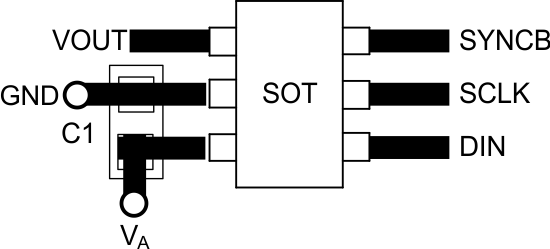
A precision analog component requires careful layout, adequate bypassing, and clean, well-regulated power supplies. The power applied to VA must be well regulated and low noise. Switching power supplies and DC/DC converters will often have high-frequency glitches or spikes riding on the output voltage. In addition, digital components can create similar high-frequency spikes as their internal logic switches states. This noise can easily couple into the DAC output voltage through various paths between the power connections and analog output. As with the GND connection, VA must be connected to a power supply plane or trace that is separate from the connection for digital logic until they are connected at the power entry point.
The DAC121S101 power supply must be bypassed with a 10-µF and a 0.1-µF capacitor as close as possible to the device with the 0.1 µF right at the device supply pin. The 10-µF capacitor must be a tantalum type and the 0.1-µF capacitor must be a low ESL, low ESR type. The power supply for the DAC121S101 must only be used for analog circuits.
For best accuracy and minimum noise, the printed-circuit-board containing the DAC121S101 must have separate analog and digital areas. The areas are defined by the locations of the analog and digital power planes. Both of these planes must be located in the same board layer. There must be a single ground plane. A single ground plane is preferred if digital return current does not flow through the analog ground area. Frequently a single ground plane design will use a fencing technique to prevent the mixing of analog and digital ground current. Separate ground planes must only be used when the fencing technique is inadequate. The separate ground planes must be connected in one place, preferably near the DAC121S101. Take special care to ensure that digital signals with fast edge rates do not pass over split ground planes. They must always have a continuous return path below their traces.
Avoid crossover of analog and digital signals and keep the clock and data lines on the component side of the board. The clock and data lines must have controlled impedances.
11.2 Layout Example
 Figure 46. Typical Layout