SNAS265J June 2005 – September 2015 DAC121S101 , DAC121S101-Q1
PRODUCTION DATA.
- 1 Features
- 2 Applications
- 3 Description
- 4 Revision History
- 5 Description continued
- 6 Pin Configuration and Functions
- 7 Specifications
- 8 Detailed Description
- 9 Application and Implementation
- 10Power Supply Recommendations
- 11Layout
- 12Device and Documentation Support
- 13Mechanical, Packaging, and Orderable Information
Package Options
Mechanical Data (Package|Pins)
Thermal pad, mechanical data (Package|Pins)
Orderable Information
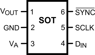
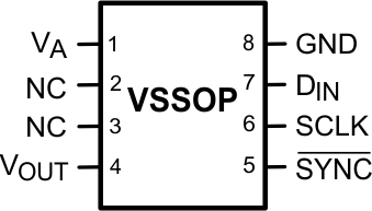
6 Pin Configuration and Functions
DDC Package
6-Pin SOT
Top View

DAC121S101 (Only) DGK Package
8-Pin VSSOP
Top View

Pin Functions
| PIN | I/O | DESCRIPTION | ||
|---|---|---|---|---|
| NAME | SOT NO. | VSSOP NO. | ||
| DIN | 4 | 7 | Input | Serial Data Input. Data is clocked into the 16-bit shift register on the falling edges of SCLK after the fall of SYNC. |
| GND | 2 | 8 | — | Ground reference for all on-chip circuitry. |
| NC | — | 2 | — | No Connect. There is no internal connection to these pins. |
| 3 | ||||
| SCLK | 5 | 6 | Input | Serial Clock Input. Data is clocked into the input shift register on the falling edges of this pin. |
| SYNC | 6 | 5 | Input | Frame synchronization input for the data input. When this pin goes low, it enables the input shift register and data is transferred on the falling edges of SCLK. The DAC is updated on the 16th clock cycle unless SYNC is brought high before the 16th clock, in which case the rising edge of SYNC acts as an interrupt and the write sequence is ignored by the DAC. |
| VA | 3 | 1 | — | Power supply and Reference input. Should be decoupled to GND. |
| VOUT | 1 | 4 | Output | DAC Analog Output Voltage. |