SNAS265J June 2005 – September 2015 DAC121S101 , DAC121S101-Q1
PRODUCTION DATA.
- 1 Features
- 2 Applications
- 3 Description
- 4 Revision History
- 5 Description continued
- 6 Pin Configuration and Functions
- 7 Specifications
- 8 Detailed Description
- 9 Application and Implementation
- 10Power Supply Recommendations
- 11Layout
- 12Device and Documentation Support
- 13Mechanical, Packaging, and Orderable Information
Package Options
Mechanical Data (Package|Pins)
Thermal pad, mechanical data (Package|Pins)
Orderable Information
10 Power Supply Recommendations
NOTE
Information in the following power supply recommendations section is not part of the TI component specification, and TI does not warrant its accuracy or completeness. TI’s customers are responsible for determining suitability of components for their purposes. Customers should validate and test their design implementation to confirm system functionality.
10.1 Using References as Power Supplies
Recall the need for a quiet supply source for devices that use their power supply voltage as a reference voltage.
Because the DAC121S101 consumes very little power, a reference source may be used as the supply voltage. The advantages of using a reference source over a voltage regulator are accuracy and stability. Some low noise regulators can also be used for the power supply of the DAC121S101. Listed below are a few power supply options for the DAC121S101.
10.1.1 LM4130
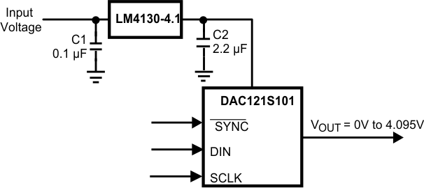
The LM4130 reference, with its 0.05% accuracy over temperature, is a good choice as a power source for the DAC121S101. Its primary disadvantage is the lack of 3-V and 5-V versions. However, the 4.096-V version is useful if a 0 to 4.095-V output range is desirable or acceptable. Bypassing the LM4130 VIN pin with a 0.1-µF capacitor and the VOUT pin with a 2.2-µF capacitor will improve stability and reduce output noise. The LM4130 comes in a space-saving 5-pin SOT23.
 Figure 42. The LM4130 as a Power Supply
10.1.2 LM4050
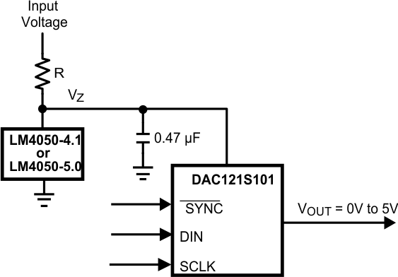
Available with accuracy of 0.44%, the LM4050 shunt reference is also a good choice as a power regulator for the DAC121S101. It does not come in a 3-V version, but 4.096-V and 5-V versions are available. It comes in a space-saving 3-pin SOT23.
 Figure 43. The LM4050 as a Power Supply
The minimum resistor value in the circuit of Figure 43 must be chosen such that the maximum current through the LM4050 does not exceed its 15-mA rating. The conditions for maximum current include the input voltage at its maximum, the LM4050 voltage at its minimum, the resistor value at its minimum due to tolerance, and the DAC121S101 draws zero current. The maximum resistor value must allow the LM4050 to draw more than its minimum current for regulation plus the maximum DAC121S101 current in full operation. The conditions for minimum current include the input voltage at its minimum, the LM4050 voltage at its maximum, the resistor value at its maximum due to tolerance, and the DAC121S101 draws its maximum current. These conditions can be summarized as
and
where
- VZ(min) and VZ(max) are the nominal LM4050 output voltages ± the LM4050 output tolerance over temperature,
- IZ(max) is the maximum allowable current through the LM4050,
- IZ(min) is the minimum current required by the LM4050 for proper regulation,
- IA(max) is the maximum DAC121S101 supply current,
- and IA(min) is the minimum DAC121S101 supply current.
10.1.3 LP3985
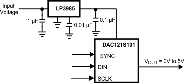
The LP3985 is a low noise, ultra-low dropout voltage regulator with a 3% accuracy over temperature. It is a good choice for applications that do not require a precision reference for the DAC121S101. It comes in 3-V, 3.3-V and 5-V versions, among others, and sports a low 30-µV noise specification at low frequencies. Because low-frequency noise is relatively difficult to filter, this specification could be important for some applications. The LP3985 comes in a space-saving 5-pin SOT-23 and 5-bump DSBGA packages.
 Figure 44. Using the LP3985 Regulator
An input capacitance of 1 µF without any ESR requirement is required at the LP3985 input, while a 1-µF ceramic capacitor with an ESR requirement of 5 mΩ to 500 mΩ is required at the output. Careful interpretation and understanding of the capacitor specification is required to ensure correct device operation.
10.1.4 LP2980
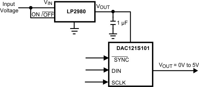
The LP2980 is an ultra-low dropout regulator with a 0.5% or 1.0% accuracy over temperature, depending upon grade. It is available in 3-V, 3.3-V and 5-V versions, among others.
 Figure 45. Using the LP2980 Regulator
Like any low dropout regulator, the LP2980 requires an output capacitor for loop stability. This output capacitor must be at least 1-µF over temperature, but values of 2.2 µF or more will provide even better performance. The ESR of this capacitor must be within the range specified in the LP2980 data sheet. Surface-mount solid tantalum capacitors offer a good combination of small size and ESR. Ceramic capacitors are attractive due to their small size but generally have ESR values that are too low for use with the LP2980. Aluminum electrolytic capacitors are typically not a good choice due to their large size and have ESR values that may be too high at low temperatures.