SBASAS1A November 2023 – March 2024 DAC39RF12 , DAC39RFS12
PRODUCTION DATA
- 1
- 1 Features
- 2 Applications
- 3 Description
- 4 Device Comparison
- 5 Pin Configuration and Functions
-
6 Specifications
- 6.1 Absolute Maximum Ratings
- 6.2 ESD Ratings
- 6.3 Recommended Operating Conditions
- 6.4 Thermal Information
- 6.5 Electrical Characteristics - DC Specifications
- 6.6 Electrical Characteristics - AC Specifications
- 6.7 Electrical Characteristics - Power Consumption
- 6.8 Timing Requirements
- 6.9 Switching Characteristics
- 6.10 SPI and FRI Timing Diagrams
- 6.11 Typical Characteristics: Bandwidth and DC Linearity
- 6.12 Typical Characteristics: Single Tone Spectra
- 6.13 Typical Characteristics: Dual Tone Spectra
- 6.14 Typical Characteristics: Noise Spectral Density
- 6.15 Typical Characteristics: Linearity Sweeps
- 6.16 Typical Characteristics: Modulated Waveforms
- 6.17 Typical Characteristics: Phase and Amplitude Noise
- 6.18 Typical Characteristics: Power Dissipation and Supply Currents
-
7 Detailed Description
- 7.1 Overview
- 7.2 Functional Block Diagrams
- 7.3
Feature Description
- 7.3.1 DAC Output Modes
- 7.3.2 DAC Core
- 7.3.3 DEM and Dither
- 7.3.4 Offset Adjustment
- 7.3.5 Clocking Subsystem
- 7.3.6 Digital Signal Processing Blocks
- 7.3.7
JESD204C Interface
- 7.3.7.1 Deviation from JESD204C Standard
- 7.3.7.2 Transport Layer
- 7.3.7.3 Scrambler and Descrambler
- 7.3.7.4 Link Layer
- 7.3.7.5 Physical Layer
- 7.3.7.6 Serdes PLL Control
- 7.3.7.7 Serdes Crossbar
- 7.3.7.8 Multi-Device Synchronization and Deterministic Latency
- 7.3.7.9 Operation in Subclass 0 Systems
- 7.3.7.10 Link Reset
- 7.3.8 Alarm Generation
- 7.4 Device Functional Modes
- 7.5 Programming
- 8 Application and Implementation
- 9 Device and Documentation Support
- 10Revision History
- 11Mechanical, Packaging, and Orderable Information
Package Options
Mechanical Data (Package|Pins)
Thermal pad, mechanical data (Package|Pins)
Orderable Information
7.3.2.1 DAC Output Structure
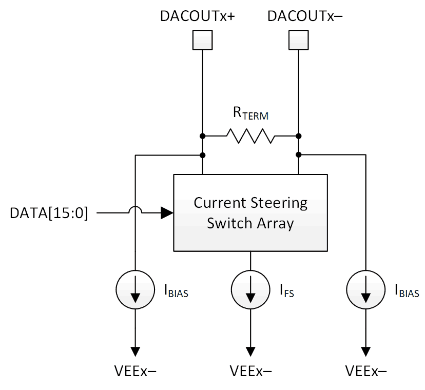
The DAC core analog output structure is shown in Figure 7-11 for one DAC channel. There is a differential termination resistance between the two current output pins, DACOUTx±. The current steering switch array connects to the output pins and steers current between the output pins based on the digital code. A constant DC current bias, IBIAS, draws current from both outputs regardless of the digital code. The IBIAS current is:
With a 3.6-kΩ resistor from RBIAS+ to RBIAS-.
 Figure 7-11 Analog Output Structure
Examples of conversions from digital codes to currents on the IOUTx± outputs are given in Table 7-2. The currents shown in Table 7-2 include both the current steered portion and the bias currents on each leg.
| DIGITAL CODE | 2'S COMPLEMENT | OFFSET BINARY | IDACOUTx+ | IDACOUTx– | IDACOUTx+ – IDACOUTx– |
|---|---|---|---|---|---|
| 32767 | 0111 1111 1111 1111 | 1111 1111 1111 1111 | 0.9999847 × IFS + IBIAS | 0.0000153 × IFS + IBIAS | 0.9999694 × IFS |
| 16384 | 0100 0000 0000 0000 | 1100 0000 0000 0000 | ¾ × IFS + IBIAS | ¼ × IFS + IBIAS | ½ × IFS |
| 0 | 0000 0000 0000 0000 | 0000 0000 0000 0000 | ½ × IFS + IBIAS | ½ × IFS + IBIAS | 0 |
| –16384 | 1100 0000 0000 0000 | 0100 0000 0000 0000 | ¼ × IFS + IBIAS | ¾ × IFS + IBIAS | –½ × IFS |
| –32768 | 1000 0000 0000 0000 | 0000 0000 0000 0000 | IBIAS | IFS + IBIAS | –IFS |