SLAS535F September 2007 – October 2018 DAC5652A
PRODUCTION DATA.
- 1 Features
- 2 Applications
- 3 Description
- 4 Revision History
- 5 Pin Configuration and Functions
-
6 Specifications
- 6.1 Absolute Maximum Ratings
- 6.2 ESD Ratings
- 6.3 Recommended Operating Conditions
- 6.4 Thermal Information
- 6.5 Electrical Characteristics: DC
- 6.6 Electrical Characteristics: AC
- 6.7 Electrical Characteristics: Digital Input
- 6.8 Electrical Characteristics: Power Supply
- 6.9 Switching Characteristics
- 6.10 Typical Characteristics
- 7 Detailed Description
- 8 Application and Implementation
- 9 Power Supply Recommendations
- 10Layout
- 11Device and Documentation Support
- 12Mechanical, Packaging, and Orderable Information
Package Options
Mechanical Data (Package|Pins)
Thermal pad, mechanical data (Package|Pins)
Orderable Information
8.1.3 Differential With Transformer
Using an RF transformer provides a convenient way of converting the differential output signal into a single-ended signal while achieving excellent dynamic performance. The appropriate transformer must be carefully selected based on the output frequency spectrum and impedance requirements.
The differential transformer configuration has the benefit of significantly reducing common-mode signals, thus improving the dynamic performance over a wide range of frequencies. Furthermore, by selecting a suitable impedance ratio (winding ratio) the transformer can provide optimum impedance matching while controlling the compliance voltage for the converter outputs.
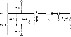
Figure 18 and Figure 19 show 50-Ω doubly-terminated transformer configurations with 1:1 and 4:1 impedance ratios, respectively. Note that the center tap of the primary input of the transformer has to be grounded to enable a dc-current flow. Applying a 20-mA full-scale output current would lead to a 0.5-VPP output for a 1:1 transformer and a 1-VPP output for a 4:1 transformer. In general, the 1:1 transformer configuration has a better output distortion, but the 4:1 transformer has 6 dB higher output power.
 Figure 18. Driving a Doubly-Terminated 50-Ω Cable Using a 1:1 Impedance Ratio Transformer
  Figure 19. Driving a Doubly-Terminated 50-Ω Cable Using a 4:1 Impedance Ratio Transformer