SLAS464C December 2006 – January 2018 DAC8560
PRODUCTION DATA.
- 1 Features
- 2 Applications
- 3 Description
- 4 Revision History
- 5 Pin Configuration and Functions
-
6 Specifications
- 6.1 Absolute Maximum Ratings
- 6.2 ESD Ratings
- 6.3 Recommended Operating Conditions
- 6.4 Thermal Information
- 6.5 Electrical Characteristics
- 6.6 Timing Requirements
- 6.7 Typical Characteristics: Internal Reference
- 6.8 Typical Characteristics: DAC at VDD = 5 V
- 6.9 Typical Characteristics: DAC at VDD = 3.6 V
- 6.10 Typical Characteristics: DAC at VDD = 2.7 V
-
7 Detailed Description
- 7.1 Overview
- 7.2 Functional Block Diagram
- 7.3 Feature Description
- 7.4 Device Functional Modes
- 7.5 Programming
- 7.6 Register Maps
- 8 Application and Implementation
- 9 Power Supply Recommendations
- 10Layout
- 11Device and Documentation Support
- 12Mechanical, Packaging, and Orderable Information
Package Options
Mechanical Data (Package|Pins)
- DGK|8
Thermal pad, mechanical data (Package|Pins)
Orderable Information
7.4.1 Power-Down Modes
The DAC8560 supports four separate modes of operation. These modes are programmable by setting two bits (PD1 and PD0) in the control register. Table 1 shows how to control the operating mode with data bits PD1 (DB17) and PD0 (DB16).
Table 1. Operating Modes
| PD1 (DB17) | PD0 (DB16) | OPERATING MODE |
|---|---|---|
| 0 | 0 | Normal operation |
| 0 | 1 | Power-down 1 kΩ to GND |
| 1 | 0 | Power-down 100 kΩ to GND |
| 1 | 1 | Power-down High-Z |
When both bits are set to 0, the device works normally with its typical current consumption of 530 μA at 5.5 V. However, for the three power-down modes, the supply current falls to 1.2 μA at 5.5 V (0.7 μA at 3.6 V). Not only does the supply current fall, but the output stage is also internally switched from the output of the amplifier to a resistor network of known values.
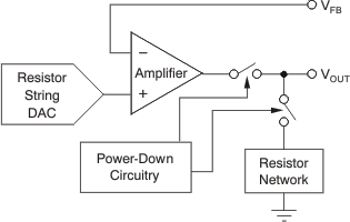
The advantage of this switching is that the output impedance of the device is known while it is in power-down mode. As shown in Table 1, there are three different power-down options. VOUT can be connected internally to GND through a 1-kΩ resistor, a 100-kΩ resistor, or open-circuited (High-Z). The output stage is shown in Figure 68.
 Figure 68. Output Stage During Power Down
 All analog circuitry is shut down when the power-down mode is activated. However, the contents of the DAC register are unaffected when in power down. The time to exit power down is typically 2.5 μs for VDD = 5 V, and 5 μs for VDD = 3 V. See the Typical Characteristics: DAC at VDD = 5 V for more information.