SLAS464C December   2006  – January 2018 DAC8560

PRODUCTION DATA.  

  1. Features
  2. Applications
  3. Description
    1.     Device Images
      1.      Functional Block Diagram
  4. Revision History
  5. Pin Configuration and Functions
    1.     Pin Functions
  6. Specifications
    1. 6.1  Absolute Maximum Ratings
    2. 6.2  ESD Ratings
    3. 6.3  Recommended Operating Conditions
    4. 6.4  Thermal Information
    5. 6.5  Electrical Characteristics
    6. 6.6  Timing Requirements
    7. 6.7  Typical Characteristics: Internal Reference
    8. 6.8  Typical Characteristics: DAC at VDD = 5 V
    9. 6.9  Typical Characteristics: DAC at VDD = 3.6 V
    10. 6.10 Typical Characteristics: DAC at VDD = 2.7 V
  7. Detailed Description
    1. 7.1 Overview
    2. 7.2 Functional Block Diagram
    3. 7.3 Feature Description
      1. 7.3.1 Digital-to-Analog Converter (DAC)
      2. 7.3.2 Resistor String
      3. 7.3.3 Output Amplifier
      4. 7.3.4 DAC Noise Performance
      5. 7.3.5 Internal Reference
        1. 7.3.5.1 Enable/Disable Internal Reference
        2. 7.3.5.2 Internal Reference Load
          1. 7.3.5.2.1 Supply Voltage
          2. 7.3.5.2.2 Temperature Drift
          3. 7.3.5.2.3 Noise Performance
          4. 7.3.5.2.4 Load Regulation
          5. 7.3.5.2.5 Long-Term Stability
          6. 7.3.5.2.6 Thermal Hysteresis
    4. 7.4 Device Functional Modes
      1. 7.4.1 Power-Down Modes
    5. 7.5 Programming
      1. 7.5.1 Serial Interface
      2. 7.5.2 Input Shift Register
      3. 7.5.3 SYNC Interrupt
      4. 7.5.4 Power-On Reset
    6. 7.6 Register Maps
      1. 7.6.1 Write Sequence for Disabling the DAC8560 Internal Reference
        1. Table 1. Write Sequence for Disabling the DAC8560 Internal Reference
      2. 7.6.2 Enabling the DAC8560 Internal Reference (Write Sequence 1 of 2)
        1. Table 2. Enabling the DAC8560 Internal Reference (Write Sequence 1 of 2)
      3. 7.6.3 Enabling the DAC8560 Internal Reference (Write Sequence 2 of 2)
        1. Table 3. Enabling the DAC8560 Internal Reference (Write Sequence 2 of 2)
      4. 7.6.4 DAC8560 Data Input Register Format
        1. Table 4. DAC8560 Data Input Register Format
  8. Application and Implementation
    1. 8.1 Application Information
    2. 8.2 Typical Applications
      1. 8.2.1 Design Requirements
      2. 8.2.2 Detailed Design Procedure or Bipolar Operation > ±VREF
        1. 8.2.2.1 Bipolar Operation Greater Than ±VREF
          1. 8.2.2.1.1 Passive Component Selection
          2. 8.2.2.1.2 Amplifier Selection
        2. 8.2.2.2 Microprocessor Interfacing
          1. 8.2.2.2.1 DAC8560 to 8051 Interface
          2. 8.2.2.2.2 DAC8560 to Microwire Interface
          3. 8.2.2.2.3 DAC8560 to 68HC11 Interface
      3. 8.2.3 Application Curves
  9. Power Supply Recommendations
  10. 10Layout
    1. 10.1 Layout Guidelines
    2. 10.2 Layout Example
  11. 11Device and Documentation Support
    1. 11.1 Documentation Support
      1. 11.1.1 Related Documentation
    2. 11.2 Receiving Notification of Documentation Updates
    3. 11.3 Community Resource
    4. 11.4 Trademarks
    5. 11.5 Electrostatic Discharge Caution
    6. 11.6 Glossary
  12. 12Mechanical, Packaging, and Orderable Information

Package Options

Mechanical Data (Package|Pins)
Thermal pad, mechanical data (Package|Pins)
Orderable Information

Typical Applications

The output voltage with Figure 70 and Figure 71 for any input code can be calculated using Equation 4:

Equation 4. DAC8560 q_vo1_las464.gif

where

    With VREF = 5 V, R1 = R2 = 10 kΩ.

    Equation 5. DAC8560 q_vo2_las464.gif

    This result has an output voltage range of ±5 V with 0000h corresponding to a –5-V output and FFFFh corresponding to a 5-V output, as shown in Figure 70. Similarly, using the internal reference, a ±2.5-V output voltage range can be achieved, as shown in Figure 71.
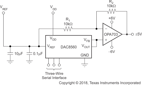
    DAC8560 ai_bipolar_ext_las464.gifFigure 70. Bipolar Output Range Using External Reference at 5 V
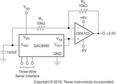
    DAC8560 ai_bipolar_int_las464.gifFigure 71. Bipolar Output Range Using Internal Reference
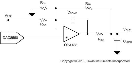
    DAC8560 bipolar-output-diagram-slas464.gifFigure 72. Bipolar Output Range > ±VREF