DLPS140B March 2019 – May 2022 DLP2000
PRODUCTION DATA
- 1 Features
- 2 Applications
- 3 Description
- 4 Revision History
- 5 Pin Configuration and Functions
-
6 Specifications
- 6.1 Absolute Maximum Ratings
- 6.2 Storage Conditions
- 6.3 ESD Ratings
- 6.4 Recommended Operating Conditions
- 6.5 Thermal Information
- 6.6 Electrical Characteristics
- 6.7 Timing Requirements
- 6.8 System Mounting Interface Loads
- 6.9 Physical Characteristics of the Micromirror Array
- 6.10 Micromirror Array Optical Characteristics
- 6.11 Window Characteristics
- 6.12 Chipset Component Usage Specification
- 7 Detailed Description
- 8 Application and Implementation
- 9 Power Supply Recommendations
- 10Layout
- 11Device and Documentation Support
- 12Mechanical, Packaging, and Orderable Information
Package Options
Mechanical Data (Package|Pins)
- FQC|42
Thermal pad, mechanical data (Package|Pins)
Orderable Information
7.6 Micromirror Array Temperature Calculation
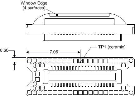
 Figure 7-1 DMD Thermal Test Point
The micromirror array temperature can be computed analytically from measurement points on the outside of the package, the package thermal resistance, the electrical power dissipation, and the illumination heat load. The relationship between array temperature and the reference ceramic temperature is provided by the following equations:
- TARRAY = Computed DMD array temperature (°C)
- TCERAMIC = Measured ceramic temperature (°C), TP1 location in Figure 7-1
- RARRAY–TO–CERAMIC = DMD package thermal resistance from array to outside ceramic (°C/W), specified in Section 6.5
- QARRAY = Total DMD power; electrical plus absorbed (calculated) (W)
- QELECTRICAL = Nominal DMD electrical power dissipation (W)
- CL2W = Conversion constant for screen lumens to absorbed optical power on the DMD (W/lm)
- SL = Measured ANSI screen lumens (lm)
The electrical power dissipation of the DMD is variable and depends on the voltages, data rates, and operating frequencies. A nominal electrical power dissipation to use when calculating array temperature is 0.045 watts. The absorbed power from the illumination source is variable and depends on the operating state of the mirrors and the intensity of the light source. The equations shown previously are valid for a 1-Chip DMD system with a total projection efficiency from DMD to screen of 87%.
The conversion constant CL2W is based on DMD micromirror array characteristics. It assumes a spectral efficiency of 300 lumens/watt for the projected light, and an illumination distribution of 83.7% on the DMD active array and 16.3% on the DMD array border and window aperture. The conversion constant is calculated to be 0.00293 W/lm.
The following is a sample calculation for a typical projection application:
- SL = 20 lm
- TCeramic = 55°C
- QArray = QELECTRICAL + QILLUMINATION = 0.045 W + (0.00293 W/lm × 20 lm) = 0.1036 W
- TArray = 55°C + (0.1036 W × 8°C/W) = 55.8°C