SNLS505G july 2016 – august 2023 DP83822H , DP83822HF , DP83822I , DP83822IF
PRODUCTION DATA
- 1
- 1 Features
- 2 Applications
- 3 Description
- 4 Revision History
- 5 Device Comparison Table
- 6 Pin Configuration and Functions
-
7 Specifications
- 7.1 Absolute Maximum Ratings
- 7.2 ESD Ratings
- 7.3 Recommended Operating Conditions
- 7.4 Thermal Information
- 7.5 Electrical Characteristics
- 7.6 Timing Requirements, Power-Up Timing
- 7.7 Timing Requirements, Power-Up With Unstable XI Clock
- 7.8 Timing Requirements, Reset Timing
- 7.9 Timing Requirements, Serial Management Timing
- 7.10 Timing Requirements, 100 Mbps MII Transmit Timing
- 7.11 Timing Requirements, 100 Mbps MII Receive Timing
- 7.12 Timing Requirements, 10 Mbps MII Transmit Timing
- 7.13 Timing Requirements, 10 Mbps MII Receive Timing
- 7.14 Timing Requirements, RMII Transmit Timing
- 7.15 Timing Requirements, RMII Receive Timing
- 7.16 Timing Requirements, RGMII
- 7.17 Normal Link Pulse Timing
- 7.18 Auto-Negotiation Fast Link Pulse (FLP) Timing
- 7.19 10BASE-Te Jabber Timing
- 7.20 100BASE-TX Transmit Latency Timing
- 7.21 100BASE-TX Receive Latency Timing
- 7.22 Timing Diagrams
- 7.23 Typical Characteristics
-
8 Detailed Description
- 8.1 Overview
- 8.2 Functional Block Diagram
- 8.3 Feature Description
- 8.4
Device Functional Modes
- 8.4.1 MAC Interfaces
- 8.4.2
Serial Management Interface
- 8.4.2.1 Extended Register Space Access
- 8.4.2.2 Write Address Operation
- 8.4.2.3 Read Address Operation
- 8.4.2.4 Write (No Post Increment) Operation
- 8.4.2.5 Read (No Post Increment) Operation
- 8.4.2.6 Write (Post Increment) Operation
- 8.4.2.7 Read (Post Increment) Operation
- 8.4.2.8 Example Write Operation (No Post Increment)
- 8.4.2.9 Example Read Operation (No Post Increment)
- 8.4.3 100BASE-TX
- 8.4.4 100BASE-FX
- 8.4.5 10BASE-Te
- 8.4.6 Auto-Negotiation (Speed / Duplex Selection)
- 8.4.7 Auto-MDIX Resolution
- 8.4.8 Loopback Modes
- 8.4.9 BIST Configurations
- 8.4.10 Cable Diagnostics
- 8.4.11 Fast Link Down Functionality
- 8.5 Programming
- 8.6 Register Maps
- 9 Application and Implementation
- 10Power Supply Recommendations
- 11Layout
- 12Device and Documentation Support
- 13Mechanical, Packaging, and Orderable Information
Package Options
Mechanical Data (Package|Pins)
- RHB|32
Thermal pad, mechanical data (Package|Pins)
- RHB|32
Orderable Information
8.5.2 LED Configuration
The DP83822 supports up to three configurable Light Emitting Diode (LED) pins: LED_0, LED_1 (GPIO1), COL (GPIO2) and RX_D3 (GPIO3). Several functions can be multiplexed onto the LEDs for different modes of operation. The LED configuration modes are selected using the LEDs Configuration Register (LEDCFG1, register 0x0460) and the Multi-LED Control Register (MLEDCR, register 0x0025). LED_0 and COL (GPIO2) use the MLED function found in register 0x0025. MLED can be routed to only one of these two pins at a time. MLED routing is determined by bits[1:0] in register 0x0025.
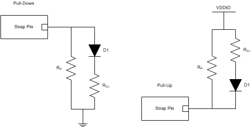
Because LED pins are also used as bootstrap pins, external components must be considered in order to avoid contention. LED pins are automatically configured for the proper polarity based on the bootstrap configuration at power up or hardware reset. If an LED pin is resistively pulled low, the corresponding output will be configured as an active high driver. Conversely, if a given bootstrap input is resistively pulled high, the corresponding output will be configured as an active low driver.
An example below shows proper bootstrap connections for LED pins using either pullup or pulldown configurations.
Note: LED_0 and LED_1 require parallel pullup or pulldown resistors when using the pin in conjunction with an LED and current limiting resistor. A 1.96kΩ to 2.49kΩ resistor should be used as the parallel pull resistor. When LED pins are not used, they can be left floating.
 Figure 8-11 Example Strap Connections