SLLSEJ7 February 2015 DP83848-HT
PRODUCTION DATA.
- 1 Features
- 2 Applications
- 3 Description
- 4 Typical System Diagram
- 5 Revision History
- 6 Bare Die Information
- 7 Specifications
-
8 Detailed Description
- 8.1 Overview
- 8.2 Functional Block Diagram
- 8.3
Feature Description
- 8.3.1 100BASE-TX Transmitter
- 8.3.2 100BASE-TX Receiver
- 8.3.3
10BASE-T Transceiver Module
- 8.3.3.1 Operational Modes
- 8.3.3.2 Smart Squelch
- 8.3.3.3 Collision Detection and SQE
- 8.3.3.4 Carrier Sense
- 8.3.3.5 Normal Link Pulse Detection/Generation
- 8.3.3.6 Jabber Function
- 8.3.3.7 Automatic Link Polarity Detection and Correction
- 8.3.3.8 Transmit and Receive Filtering
- 8.3.3.9 Transmitter
- 8.3.3.10 Receiver
- 8.3.4 Reset Operation
- 8.4 Device Functional Modes
- 8.5 Programming
- 8.6
Register Maps
- 8.6.1 Register Block
- 8.6.2
Register Definition
- 8.6.2.1 Basic Mode Control Register (BMCR)
- 8.6.2.2 Basic Mode Status Register (BMSR)
- 8.6.2.3 PHY Identifier Register 1 (PHYIDR1)
- 8.6.2.4 PHY Identifier Register 2 (PHYIDR2)
- 8.6.2.5 Auto-Negotiation Advertisement Register (ANAR)
- 8.6.2.6 Auto-Negotiation Link Partner Ability Register (ANLPAR) (BASE Page)
- 8.6.2.7 Auto-Negotiation Link Partner Ability Register (ANLPAR) (Next Page)
- 8.6.2.8 Auto-Negotiate Expansion Register (ANER)
- 8.6.2.9 Auto-Negotiation Next Page Transmit Register (ANNPTR)
- 8.6.3
Extended Registers
- 8.6.3.1 PHY Status Register (PHYSTS)
- 8.6.3.2 MII Interrupt Control Register (MICR)
- 8.6.3.3 MII Interrupt Status and Miscellaneous Control Register (MISR)
- 8.6.3.4 False Carrier Sense Counter Register (FCSCR)
- 8.6.3.5 Receiver Error Counter Register (RECR)
- 8.6.3.6 100 Mb/s PCS Configuration and Status Register (PCSR)
- 8.6.3.7 RMII and Bypass Register (RBR)
- 8.6.3.8 LED Direct Control Register (LEDCR)
- 8.6.3.9 PHY Control Register (PHYCR)
- 8.6.3.10 10Base-T Status/Control Register (10BTSCR)
- 8.6.3.11 CD Test and BIST Extensions Register (CDCTRL1)
- 8.6.3.12 Energy Detect Control (EDCR)
- 9 Application and Implementation
- 10Power Supply Recommendations
- 11Layout
- 12Device and Documentation Support
- 13Mechanical, Packaging, and Orderable Information
Package Options
Mechanical Data (Package|Pins)
- KGD|0
Thermal pad, mechanical data (Package|Pins)
Orderable Information
6 Bare Die Information
| DIE THICKNESS | BACKSIDE FINISH | BACKSIDE POTENTIAL | BOND PAD METALLIZATION COMPOSITION | BOND PAD THICKNESS |
|---|---|---|---|---|
| 10.5 mils | Silicon with backgrind | Ground | AlCu.5% | 0.9 µm |
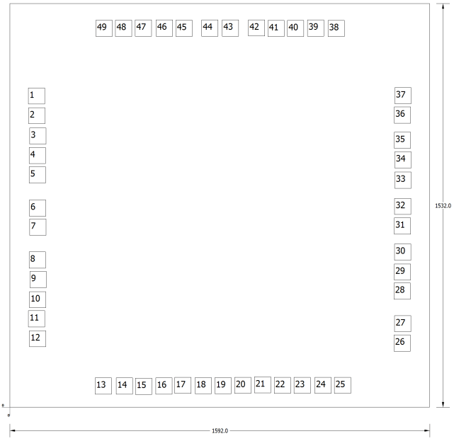
Bond Pin Coordinates in Microns
| DESCRIPTION | PAD NUMBER | X MIN | Y MIN | X MAX | Y MAX |
|---|---|---|---|---|---|
| TX_CLK | 1 | 70.339 | 1149.962 | 133.368 | 1212.499 |
| TX_EN | 2 | 71.466 | 1074.524 | 134.495 | 1137.061 |
| TXD_0 | 3 | 74.847 | 997.96 | 137.875 | 1060.497 |
| TXD_1 | 4 | 72.593 | 923.648 | 135.621 | 986.185 |
| TXD_2 | 5 | 72.593 | 850.461 | 135.621 | 912.998 |
| TXD_3/SNI_MODE | 6 | 73.72 | 724.356 | 136.748 | 786.893 |
| PWR_DOWN/INT | 7 | 74.847 | 652.295 | 137.875 | 714.832 |
| TCK | 8 | 72.812 | 527.247 | 135.841 | 589.783 |
| TDO | 9 | 75.657 | 453.341 | 138.686 | 515.878 |
| TMS | 10 | 74.235 | 376.592 | 137.263 | 439.129 |
| TRST | 11 | 69.967 | 304.108 | 132.996 | 366.645 |
| TDI | 12 | 74.235 | 228.781 | 137.263 | 291.318 |
| RD- | 13 | 322.955 | 49.09 | 385.984 | 111.627 |
| RD+ | 14 | 402.74 | 49.09 | 465.768 | 111.627 |
| AGND | 15 | 476.319 | 48.204 | 539.348 | 110.741 |
| AGND | 16 | 553.445 | 49.09 | 616.473 | 111.627 |
| TD- | 17 | 625.251 | 51.748 | 688.279 | 114.285 |
| TD+ | 18 | 702.376 | 50.862 | 765.405 | 113.399 |
| PFBIN1 | 19 | 776.842 | 50.862 | 839.87 | 113.399 |
| AGND | 20 | 852.194 | 51.748 | 915.223 | 114.285 |
| RESERVED | 21 | 927.068 | 53.532 | 990.096 | 116.069 |
| RESERVED | 22 | 1001.534 | 51.76 | 1064.562 | 114.297 |
| AVDD33 | 23 | 1076.886 | 51.76 | 1139.914 | 114.297 |
| PFBOUT | 24 | 1155.784 | 51.76 | 1218.813 | 114.297 |
| RBIAS | 25 | 1230.25 | 51.76 | 1293.279 | 114.297 |
| 25MHz_OUT | 26 | 1455.826 | 212.106 | 1518.855 | 274.643 |
| LED_ACT/COL/AN_EN | 27 | 1457.926 | 285.53 | 1520.954 | 348.067 |
| LED_SPEED/AN1 | 28 | 1455.826 | 409.302 | 1518.855 | 471.839 |
| LED_LINK/AN0 | 29 | 1457.291 | 481.851 | 1520.319 | 544.388 |
| RESET_N | 30 | 1457.99 | 557.373 | 1521.019 | 619.91 |
| MDIO | 31 | 1456.591 | 655.971 | 1519.619 | 718.508 |
| MDC | 32 | 1457.99 | 730.794 | 1521.019 | 793.331 |
| IOVDD33 | 33 | 1458.752 | 830.293 | 1521.781 | 892.83 |
| X2 | 34 | 1458.752 | 907.287 | 1521.781 | 969.824 |
| X1 | 35 | 1457.18 | 981.924 | 1520.208 | 1044.461 |
| IOGND | 36 | 1457.18 | 1076.987 | 1520.208 | 1139.524 |
| DGND | 37 | 1458.769 | 1150.513 | 1521.797 | 1213.05 |
| PFBIN2 | 38 | 1205.966 | 1405.764 | 1268.995 | 1468.301 |
| RX_CLK | 39 | 1127.754 | 1407.005 | 1190.782 | 1469.542 |
| RX_DV/MII_MODE | 40 | 1052.024 | 1405.764 | 1115.053 | 1468.301 |
| CRS/CRS_DV/LED_CFG | 41 | 978.157 | 1405.764 | 1041.185 | 1468.301 |
| RX_ER/MDIX_EN | 42 | 903.668 | 1407.625 | 966.697 | 1470.162 |
| COL/PHYAD0 | 43 | 804.841 | 1407.148 | 867.869 | 1469.685 |
| RXD_0/PHYAD1 | 44 | 727.429 | 1407.148 | 790.457 | 1469.685 |
| RXD_1/PHYAD2 | 45 | 629.094 | 1406.451 | 692.123 | 1468.988 |
| RXD_2/PHYAD3 | 46 | 554.472 | 1407.148 | 617.5 | 1469.685 |
| RXD_3/PHYAD4 | 47 | 474.967 | 1407.148 | 537.996 | 1469.685 |
| IOGND | 48 | 399.647 | 1406.451 | 462.676 | 1468.988 |
| IOVDD33 | 49 | 326.42 | 1406.451 | 389.448 | 1468.988 |