SLLSEJ7 February 2015 DP83848-HT
PRODUCTION DATA.
- 1 Features
- 2 Applications
- 3 Description
- 4 Typical System Diagram
- 5 Revision History
- 6 Bare Die Information
- 7 Specifications
-
8 Detailed Description
- 8.1 Overview
- 8.2 Functional Block Diagram
- 8.3
Feature Description
- 8.3.1 100BASE-TX Transmitter
- 8.3.2 100BASE-TX Receiver
- 8.3.3
10BASE-T Transceiver Module
- 8.3.3.1 Operational Modes
- 8.3.3.2 Smart Squelch
- 8.3.3.3 Collision Detection and SQE
- 8.3.3.4 Carrier Sense
- 8.3.3.5 Normal Link Pulse Detection/Generation
- 8.3.3.6 Jabber Function
- 8.3.3.7 Automatic Link Polarity Detection and Correction
- 8.3.3.8 Transmit and Receive Filtering
- 8.3.3.9 Transmitter
- 8.3.3.10 Receiver
- 8.3.4 Reset Operation
- 8.4 Device Functional Modes
- 8.5 Programming
- 8.6
Register Maps
- 8.6.1 Register Block
- 8.6.2
Register Definition
- 8.6.2.1 Basic Mode Control Register (BMCR)
- 8.6.2.2 Basic Mode Status Register (BMSR)
- 8.6.2.3 PHY Identifier Register 1 (PHYIDR1)
- 8.6.2.4 PHY Identifier Register 2 (PHYIDR2)
- 8.6.2.5 Auto-Negotiation Advertisement Register (ANAR)
- 8.6.2.6 Auto-Negotiation Link Partner Ability Register (ANLPAR) (BASE Page)
- 8.6.2.7 Auto-Negotiation Link Partner Ability Register (ANLPAR) (Next Page)
- 8.6.2.8 Auto-Negotiate Expansion Register (ANER)
- 8.6.2.9 Auto-Negotiation Next Page Transmit Register (ANNPTR)
- 8.6.3
Extended Registers
- 8.6.3.1 PHY Status Register (PHYSTS)
- 8.6.3.2 MII Interrupt Control Register (MICR)
- 8.6.3.3 MII Interrupt Status and Miscellaneous Control Register (MISR)
- 8.6.3.4 False Carrier Sense Counter Register (FCSCR)
- 8.6.3.5 Receiver Error Counter Register (RECR)
- 8.6.3.6 100 Mb/s PCS Configuration and Status Register (PCSR)
- 8.6.3.7 RMII and Bypass Register (RBR)
- 8.6.3.8 LED Direct Control Register (LEDCR)
- 8.6.3.9 PHY Control Register (PHYCR)
- 8.6.3.10 10Base-T Status/Control Register (10BTSCR)
- 8.6.3.11 CD Test and BIST Extensions Register (CDCTRL1)
- 8.6.3.12 Energy Detect Control (EDCR)
- 9 Application and Implementation
- 10Power Supply Recommendations
- 11Layout
- 12Device and Documentation Support
- 13Mechanical, Packaging, and Orderable Information
Package Options
Mechanical Data (Package|Pins)
- KGD|0
Thermal pad, mechanical data (Package|Pins)
Orderable Information
11 Layout
11.1 Layout Guidelines
- Place the 49.9-Ω,1% resistors, and 0.1-μF decoupling capacitor, near the PHYTER TD± and RD± pins and via directly to the Vdd plane.
- Stubs should be avoided on all signal traces, especially the differential signal pairs. See Figure 48.
- Within the pairs (for example, TD+ and TD–) the trace lengths should be run parallel to each other and matched in length. Matched lengths minimize delay differences, avoiding an increase in common mode noise and increased EMI. See Figure 48.
- All high speed data signal should have 50-Ω controlled impedance, or 100-Ω differential controlled impedance for differential signal pairs. Ideally there should be no crossover or via on the signal paths. Vias present impedance discontinuities and should be minimized. Route an entire trace or trace pair on a single layer if possible.
- Signal traces should not be run such that they cross a plane split. See Figure 9-2. A signal crossing a plane split may cause unpredictable return path currents and would likely impact signal quality as well, potentially creating EMI problems.
- Medium Dependent Interface (MDI) signal traces should have 50-Ω to ground or 100-Ω differential controlled impedance.
- To reduce digital signal energy, 50-Ω series termination resistors are recommended for all MII output signals (including RXCLK, TXCLK, and RX Data signals.)
- PCB trace lengths should be kept as short as possible. Ideally, keep the traces under 6 inches.
- Trace length matching, to within 2 inches on the MII or RMII bus is also recommended. Significant differences in the trace lengths can cause data timing issues.
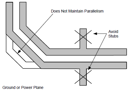 Figure 48. Differential Signal Pail - Stubs
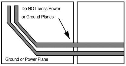 Figure 49. Differential Signal Pair-Plane Crossing
11.1.1 PCB Layer Stacking
To meet signal integrity and performance requirements, at minimum a four layer PCB is recommended for implementing PHYTER components in end user systems. The following layer stack-ups are recommended for four, six, and eight-layer boards, although other options are possible.
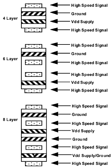 Figure 50. PCB Stripline Layer Stacking
Within a PCB it may be desirable to run traces using different methods, microstrip vs. stripline, depending on the location of the signal on the PCB. For example, it may be desirable to change layer stacking where an isolated chassis ground plane is used. Figure 51 illustrates alternative PCB stacking options.
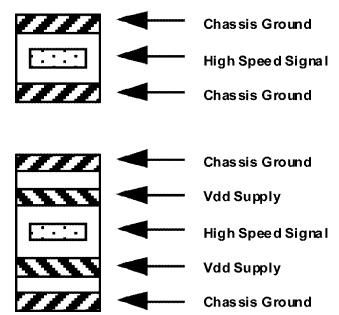 Figure 51. Alternative PCB Stripline Layer Stacking
11.2 Layout Example
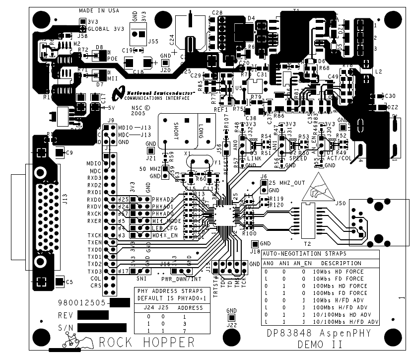 Figure 52. Top Layer
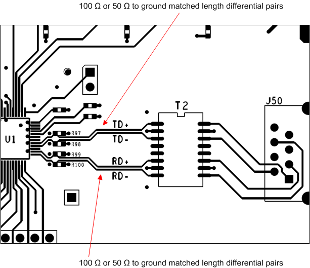 Figure 53. Differential Pairs
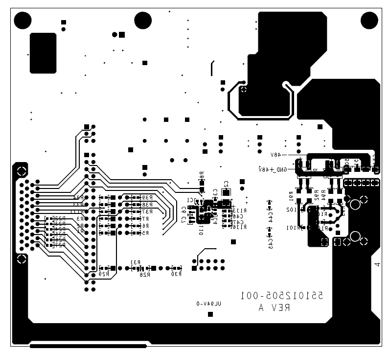 Figure 54. Bottom Layer
11.3 ESD Protection
Typically, ESD precautions are predominantly in effect when handling the devices or board before being installed in a system. In those cases, strict handling procedures need be implemented during the manufacturing process to greatly reduce the occurrences of catastrophic ESD events. After the system is assembled, internal components are less sensitive from ESD events.
See ESD Ratings for ESD rating.