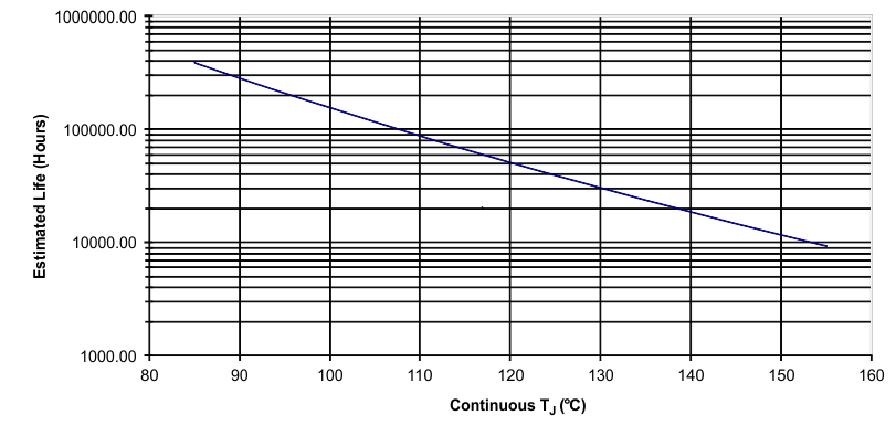
7.2 ESD Ratings
|
VALUE |
UNIT |
| V(ESD) |
ESD rating
(RZAP = 1.5 kΩ,
CZAP = 100 pF) |
Human body model (HBM), per ANSI/ESDA/JEDEC JS-001, all pins(1) |
±4000 |
V |
| Charged device model (CDM), per JEDEC specification JESD22-C101, all pins(2) |
±1000 |
(1) JEDEC document JEP155 states that 500-V HBM allows safe manufacturing with a standard ESD control process.
(2) JEDEC document JEP157 states that 250-V CDM allows safe manufacturing with a standard ESD control process.
7.3 Recommended Operating Conditions(1)
over operating free-air temperature range (unless otherwise noted)
|
MIN |
NOM |
MAX |
UNIT |
| VCC |
Supply voltage |
3 |
|
3.6 |
V |
| TA |
Operating free-air temperature(2) |
–55 |
|
150 |
°C |
| PD |
Power dissipation |
|
267 |
|
mW |
(1) Absolute maximum ratings are those values beyond which the safety of the device cannot be guaranteed. They are not meant to imply that the device should be operated at these limits.
(2) Provided that Thermal Pad is soldered down.
7.6 AC Timing Specifications
Table 1. Power-Up Timing
| PARAMETER |
NOTES |
MIN |
TYP |
MAX |
UNIT |
| T2.1.1 |
Post power-up stabilization time prior to MDC preamble for register accesses |
MDIO is pulled high for 32-bit serial management initialization |
167 |
|
|
ms |
| X1 Clock must be stable for a minimum of 167 ms at power up. |
| T2.1.2 |
Hardware configuration latching time from power up |
Hardware Configuration Pins are described in the Pin Description section |
167 |
|
|
ms |
| X1 Clock must be stable for a minimum of 167 ms at power up. |
| T2.1.3 |
Hardware configuration pins transition to output drivers |
|
|
50 |
|
ns |
Table 2. Reset Timing
| PARAMETER |
NOTES(1) |
MIN |
TYP |
MAX |
UNIT |
| T2.2.1 |
Post RESET Stabilization time prior to MDC preamble for register accesses |
MDIO is pulled high for 32-bit serial management initialization |
|
3 |
|
µs |
| T2.2.2 |
Hardware configuration latching time from the deassertion of RESET (either soft or hard) |
|
|
3 |
|
µs |
| T2.2.3 |
Hardware configuration pins transition to output drivers |
|
|
50 |
|
ns |
| T2.2.4 |
RESET pulse width |
X1 Clock must be stable for at minimum of 1 µs during RESET pulse low time |
1 |
|
|
µs |
(1) It is important to choose pull-up and/or pull-down resistors for each of the hardware configuration pins that provide fast RC time constants in order to latch-in the proper value prior to the pin transitioning to an output driver.
Table 3. MII Serial Management Timing
| PARAMETER |
NOTES |
MIN |
TYP |
MAX |
UNIT |
| T2.3.1 |
MDC to MDIO (output) delay time |
|
0 |
|
30 |
ns |
| T2.3.2 |
MDIO (input) to MDC setup time |
|
10 |
|
|
ns |
| T2.3.3 |
MDIO (input) to MDC hold time |
|
10 |
|
|
ns |
| T2.3.4 |
MDC frequency |
|
|
2.5 |
25 |
MHz |
Table 4. 100 Mb/s MII Transmit Timing
| PARAMETER |
NOTES |
MIN |
TYP |
MAX |
UNIT |
| T2.4.1 |
TX_CLK high/low time |
100 Mb/s normal mode |
16 |
20 |
24 |
ns |
| T2.4.2 |
TXD[3:0], TX_EN data setup to TX_CLK |
100 Mb/s normal mode |
9.70 |
|
|
ns |
| T2.4.3 |
TXD[3:0], TX_EN data hold from TX_CLK |
100 Mb/s normal mode |
0 |
|
|
ns |
Table 5. 100 Mb/s MII Receive Timing
| PARAMETER |
NOTES |
MIN |
TYP |
MAX |
UNIT |
| T2.5.1 |
RX_CLK high/low time |
100 Mb/s normal mode |
13 |
20 |
24 |
ns |
| T2.5.2 |
RX_CLK to RXD[3:0], RX_DV, RX_ER delay |
100 Mb/s normal mode |
|
20 |
|
ns |
Table 6. 100BASE-TX Transmit Packet Latency Timing
| PARAMETER |
NOTES(1) |
MIN |
TYP |
MAX |
UNIT |
| T2.6.1 |
TX_CLK to PMD output pair latency |
100 Mb/s normal mode |
|
6 |
|
bits |
(1) For Normal mode, latency is determined by measuring the time from the first rising edge of TX_CLK occurring after the assertion of TX_EN to the first bit of the “J” code group as output from the PMD Output Pair. 1 bit time = 10 ns in 100 Mb/s mode.
Table 7. 100BASE-TX Transmit Packet Deassertion Timing
| PARAMETER |
NOTES(1) |
MIN |
TYP |
MAX |
UNIT |
| T2.7.1 |
TX_CLK to PMD output pair deassertion |
100 Mb/s normal mode |
|
6 |
|
bits |
Table 8. 100BASE-TX Transmit Timing (tR/F & Jitter)
| PARAMETER |
NOTES(1)(2) |
MIN |
TYP |
MAX |
UNIT |
| T2.8.1 |
100 Mb/s PMD output pair tR and tF |
|
2.6 |
4 |
5.5 |
ns |
| 100 Mb/s tR and tF mismatch |
|
|
710 |
ps |
| T2.8.2(3) |
100 Mb/s PMD output pair transmit jitter |
|
|
|
1.4 |
ns |
(1) Normal Mismatch is the difference between the maximum and minimum of all rise and fall times.
(2) Rise and fall times taken at 10% and 90% of the +1 or –1 amplitude.
(3) Specified from –40°C to 125°C.
Table 9. 100BASE-TX Receive Packet Latency Timing
| PARAMETER(1) |
NOTES(2)(3) |
MIN |
TYP |
MAX |
UNIT |
| T2.9.1 |
Carrier sense ON delay |
100 Mb/s normal mode |
|
20 |
|
bits |
| T2.9.2 |
Receive data latency |
100 Mb/s normal mode |
|
24 |
|
bits |
(1) Carrier sense ON delay is determined by measuring the time from the first bit of the “J” code group to the assertion of Carrier Sense.
(2) 1 bit time = 10 ns in 100 Mb/s mode.
(3) PMD input pair voltage amplitude is greater than the signal detect turn-on threshold value.
Table 10. 100BASE-TX Receive Packet Deassertion Timing
| PARAMETER |
NOTES(1)(2) |
MIN |
TYP |
MAX |
UNIT |
| T2.10.1 |
Carrier sense OFF delay |
100 Mb/s normal mode |
|
24 |
|
bits |
(1) Carrier sense off delay is determined by measuring the time from the first bit of the “T” code group to the deassertion of carrier sense.
(2) 1 bit time = 10 ns in 100 Mb/s mode
Table 11. 10 Mb/s MII Transmit Timing
| PARAMETER |
NOTES(1) |
MIN |
TYP |
MAX |
UNIT |
| T2.11.1 |
TX_CLK high/low time |
10 Mb/s MII mode |
160 |
200 |
240 |
ns |
| T2.11.2 |
TXD[3:0], TX_EN data setup to TX_CLK fall |
10 Mb/s MII mode |
24.70 |
|
|
ns |
| T2.11.3 |
TXD[3:0], TX_EN data hold from TX_CLK rise |
10 Mb/s MII mode |
0 |
|
|
ns |
(1) An attached Mac should drive the transmit signals using the positive edge of TX_CLK. As shown above, the MII signals are sampled on the falling edge of TX_CLK.
Table 12. 10 Mb/s MII Receive Timing
| PARAMETER |
NOTES(1) |
MIN |
TYP |
MAX |
UNIT |
| T2.12.1 |
RX_CLK high/low time |
|
130 |
200 |
240 |
ns |
| T2.12.2 |
RX_CLK to RXD[3:0], RX_DV delay |
10 Mb/s MII mode |
100 |
|
|
ns |
| T2.12.3 |
RX_CLK rising edge delay from RXD[3:0], RX_DV valid |
10 Mb/s MII mode |
|
245 |
|
ns |
(1) RX_CLK may be held low for a longer period of time during transition between reference and recovered clocks. Minimum high and low times will not be violated.
Table 13. 10 Mb/s Serial Mode Transmit Timing
| PARAMETER |
NOTES |
MIN |
TYP |
MAX |
UNIT |
| T2.13.1 |
TX_CLK high time |
10 Mb/s serial mode |
|
25 |
|
ns |
| T2.13.2 |
TX_CLK low time |
10 Mb/s serial mode |
|
75 |
|
ns |
| T2.13.3 |
TXD_0, TX_EN data setup to TX_CLK rise |
10 Mb/s serial mode |
|
24.70 |
|
ns |
| T2.13.4 |
TXD_0, TX_EN data hold from TX_CLK rise |
10 Mb/s serial mode |
|
6 |
|
ns |
Table 14. 10 Mb/s Serial Mode Receive Timing
| PARAMETER |
NOTES(1) |
MIN |
TYP |
MAX |
UNIT |
| T2.14.1 |
RX_CLK high/low time |
|
|
50 |
|
ns |
| T2.14.2 |
RX_CLK fall to RXD_0, RX_DV delay |
10 Mb/s serial mode |
|
0 |
|
ns |
(1) RX_CLK may be held high for a longer period of time during transition between reference and recovered clocks. Minimum high and low times will not be violated.
Table 15. 10BASE-T Transmit Timing (Start of Packet)
| PARAMETER |
NOTES |
MIN |
TYP |
MAX |
UNIT |
| T2.15.1 |
Transmit output delay from the falling edge of TX_CLK |
10 Mb/s MII mode |
|
3.5 |
|
bits |
| T2.15.2 |
Transmit output delay from the rising edge of TX_CLK |
10 Mb/s Serial mode |
|
3.5 |
|
bits |
Table 16. 10BASE-T Transmit Timing (End of Packet)
| PARAMETER |
NOTES |
MIN |
TYP |
MAX |
UNIT |
| T2.16.1 |
End of packet high time (with ‘0’ ending bit) |
|
|
300 |
|
ns |
| T2.16.2 |
End of packet high time (with ‘1’ ending bit) |
|
|
300 |
|
ns |
Table 17. 10BASE-T Receive Timing (Start of Packet)
| PARAMETER |
NOTES(1)(2) |
MIN |
TYP |
MAX |
UNIT |
| T2.17.1 |
Carrier sense turn on delay (PMD input pair to CRS) |
|
|
630 |
1000 |
ns |
| T2.17.2 |
RX_DV latency |
|
|
10 |
|
bits |
| T2.17.3 |
Receive data latency |
Measurement shown from SFD |
|
8 |
|
bits |
(1) 10BASE-T RX_DV Latency is measured from first bit of preamble on the wire to the assertion of RX_DV
(2) 1 bit time = 100 ns in 10 Mb/s mode.
Table 18. 10BASE-T Receive Timing (End of Packet)
| PARAMETER |
NOTES |
MIN |
TYP |
MAX |
UNIT |
| T2.18.1 |
Carrier sense turn off delay |
|
|
|
1 |
µs |
Table 19. 10 Mb/s Heartbeat Timing
| PARAMETER |
NOTES |
MIN |
TYP |
MAX |
UNIT |
| T2.19.1 |
CD heartbeat delay |
All 10 Mb/s modes |
|
1200 |
|
ns |
| T2.19.2 |
CD heartbeat duration |
All 10 Mb/s modes |
|
1000 |
|
ns |
Table 20. 10 Mb/s Jabber Timing
| PARAMETER |
NOTES |
MIN |
TYP |
MAX |
UNIT |
| T2.20.1 |
Jabber activation time |
|
|
85 |
|
ms |
| T2.20.2 |
Jabber deactivation time |
|
|
500 |
|
ms |
Table 21. 10BASE-T Normal Link Pulse Timing
| PARAMETER |
NOTES(1) |
MIN |
TYP |
MAX |
UNIT |
| T2.21.1 |
Pulse width |
|
|
100 |
|
ns |
| T2.21.2 |
Pulse period |
|
|
16 |
|
ms |
(1) These specifications represent transmit timings.
Table 22. Auto-Negotiation Fast Link Pulse (FLP) Timing
| PARAMETER |
NOTES |
MIN |
TYP |
MAX |
UNIT |
| T2.22.1 |
Clock, data pulse width |
|
|
100 |
|
ns |
| T2.22.2 |
Clock pulse to clock pulse period |
|
|
125 |
|
μs |
| T2.22.3 |
Clock pulse to data pulse period |
Data = 1 |
|
62 |
|
μs |
| T2.22.4 |
Burst width |
|
|
2 |
|
ms |
| T2.22.5 |
FLP burst to FLP burst period |
|
|
16 |
|
ms |
Table 23. 100BASE-TX Signal Detect Timing
| PARAMETER |
NOTES(1) |
MIN |
TYP |
MAX |
UNIT |
| T2.23.1 |
SD internal turn-on time |
|
|
1 |
|
ms |
| T2.23.2 |
SD internal turn-off time |
|
|
350 |
|
µs |
(1) The signal amplitude on PMD Input Pair must be TP-PMD compliant.
Table 24. 100 Mb/s Internal Loopback Timing
| PARAMETER |
NOTES(1)(2) |
MIN |
TYP |
MAX |
UNIT |
| T2.24.1 |
TX_EN to RX_DV loopback |
100 Mb/s internal loopback mode |
|
240 |
|
ns |
(1) Due to the nature of the descrambler function, all 100BASE-TX Loopback modes will cause an initial “dead-time” of up to 550 μs during which time no data will be present at the receive MII outputs. The 100BASE-TX timing specified is based on device delays after the initial 550μs “dead-time”.
(2) Measurement is made from the first rising edge of TX_CLK after assertion of TX_EN.
Table 25. 10 Mb/s Internal Loopback Timing
| PARAMETER |
NOTES(1) |
MIN |
TYP |
MAX |
UNIT |
| T2.25.1 |
TX_EN to RX_DV loopback |
10 Mb/s internal loopback mode |
|
|
2.4 |
µs |
(1) Measurement is made from the first rising edge of TX_CLK after assertion of TX_EN.
Table 26. RMII Transmit Timing
| PARAMETER |
NOTES |
MIN |
TYP |
MAX |
UNIT |
| T2.26.1 |
X1 clock period |
50-MHz reference clock |
|
20 |
|
ns |
| T2.26.2 |
TXD[1:0], TX_EN, data setup to X1 rising |
|
|
3.70 |
|
ns |
| T2.26.3 |
TXD[1:0], TX_EN, data hold from X1 rising |
|
|
1.70 |
|
ns |
| T2.26.4 |
X1 clock to PMD output pair latency |
From X1 rising edge to first bit of symbol |
|
17 |
|
bits |
Table 27. RMII Receive Timing
| PARAMETER |
NOTES(1)(2)(3) |
MIN |
TYP |
MAX |
UNIT |
| T2.27.1 |
X1 clock period |
50 MHz Reference Clock |
|
20 |
|
ns |
| T2.27.2 |
RXD[1:0], CRS_DV, RX_DV and RX_ER output delay from X1 rising |
|
|
6 |
|
ns |
| T2.27.3 |
CRS ON delay |
From JK symbol on PMD receive pair to initial assertion of CRS_DV |
|
18.5 |
|
bits |
| T2.27.4 |
CRS OFF delay |
From TR symbol on PMD receive pair to initial deassertion of CRS_DV |
|
27 |
|
bits |
| T2.27.5 |
RXD[1:0] and RX_ER latency |
From symbol on receive pair. Elasticity buffer set to default value (01). |
|
38 |
|
bits |
(1) Per the RMII Specification, output delays assume a 25-pF load.
(2) CRS_DV is asserted asynchronously in order to minimize latency of control signals through the why. CRS_DV may toggle synchronously at the end of the packet to indicate CRS deassertion.
(3) RX_DV is synchronous to X1. While not part of the RMII specification, this signal is provided to simplify recovery of receive data.
Table 28. Isolation Timing
| PARAMETER |
NOTES |
MIN |
TYP |
MAX |
UNIT |
| T2.28.1 |
From software clear of bit 10 in the BMCR register to the transition from Isolate to Normal Mode |
|
|
100 |
|
µs |
| T2.28.2 |
From deassertion of software or hardware reset to transition from isolate to normal mode |
|
|
500 |
|
µs |
Table 29. 25 MHz_OUT Timing
| PARAMETER |
NOTES(1) |
MIN |
TYP |
MAX |
UNIT |
| T2.29.1 |
25 MHz_OUT high/low time |
MII mode |
|
20 |
|
ns |
| RMII mode |
|
10 |
|
| T2.29.2 |
25 MHz_OUT propagation delay |
Relative to X1 |
|
|
8 |
ns |
(1) 25 MHz_OUT characteristics are dependent upon the X1 input characteristics.
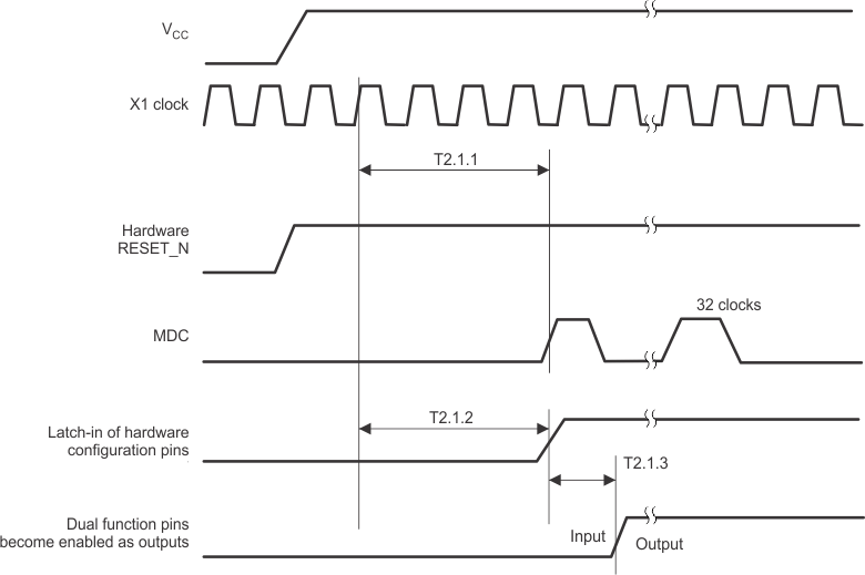 Figure 1. Power-Up Timing
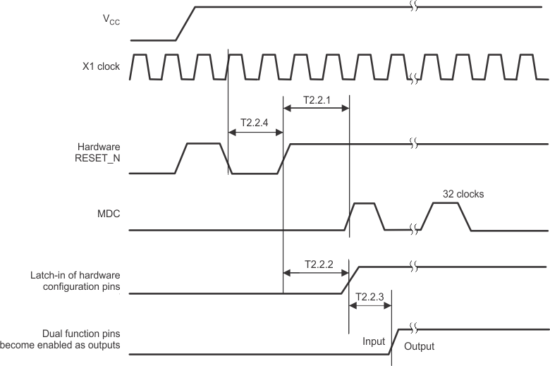 Figure 2. Reset Timing
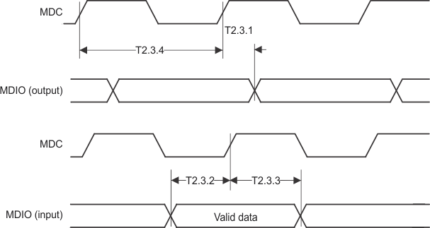 Figure 3. MII Serial Management Timing
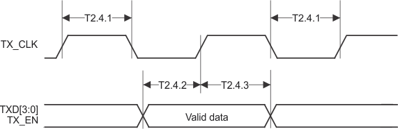 Figure 4. 100 Mb/s MII Transmit Timing
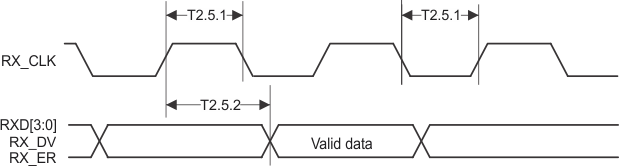 Figure 5. 100 Mb/s MII Receive Timing
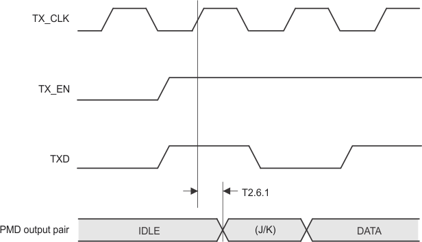 Figure 6. 100BASE-TX Transmit Packet Latency Timing
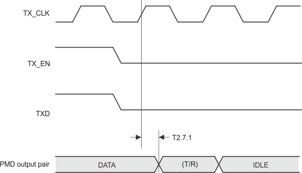 Figure 7. 100BASE-TX Transmit Packet Deassertion Timing
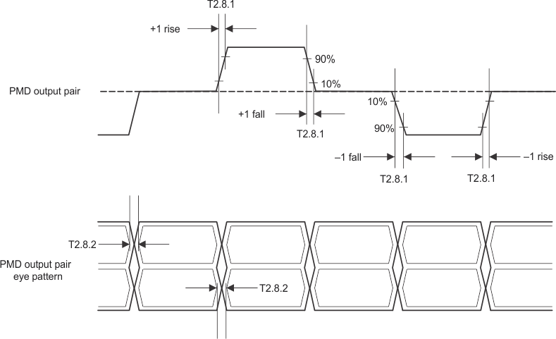 Figure 8. 100BASE-TX Transmit Timing (tR/F and Jitter)
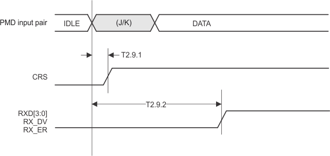 Figure 9. 100BASE-TX Receive Packet Latency Timing
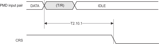 Figure 10. 100BASE-TX Receive Packet Deassertion Timing
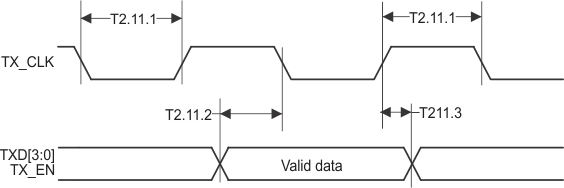 Figure 11. 10 Mb/s MII Transmit Timing
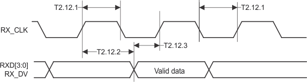 Figure 12. 10 Mb/s MII Receive Timing
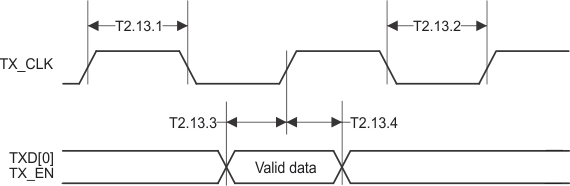 Figure 13. 10 Mb/s Serial Mode Transmit Timing
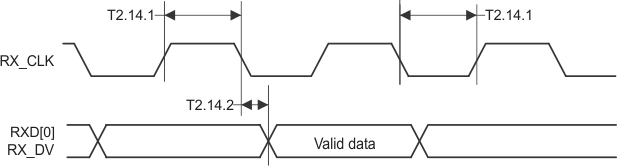 Figure 14. 10 Mb/s Serial Mode Receive Timing
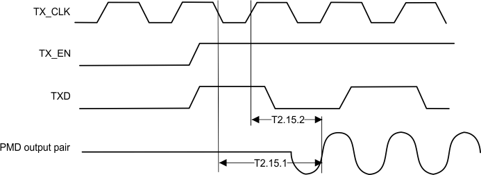 Figure 15. 10BASE-T Transmit Timing (Start of Packet)
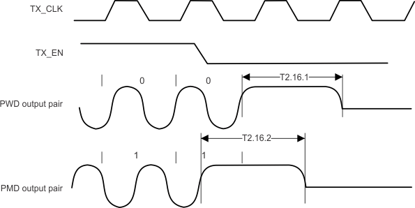 Figure 16. 10BASE-T Transmit Timing (End of Packet)
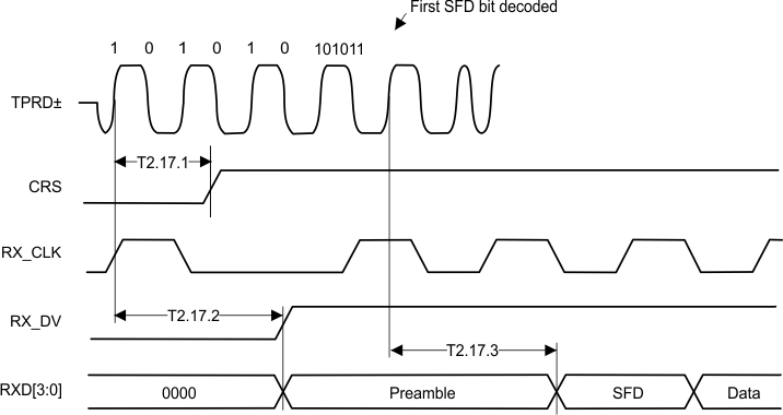 Figure 17. 10BASE-T Receive Timing (Start of Packet)
 Figure 18. 10BASE-T Receive Timing (End of Packet)
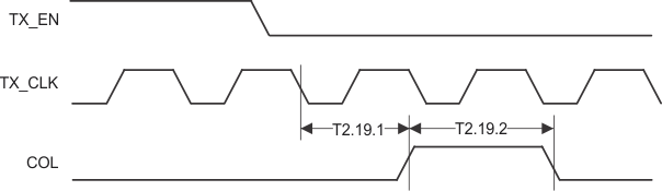 Figure 19. 10 Mb/s Heartbeat Timing
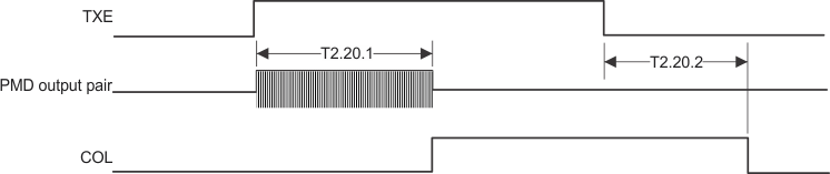 Figure 20. 10 Mb/s Jabber Timing
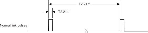 Figure 21. 10BASE-T Normal Link Pulse Timing
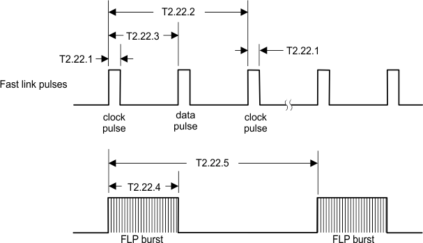 Figure 22. Auto-Negotiation Fast Link Pulse (FLP) Timing
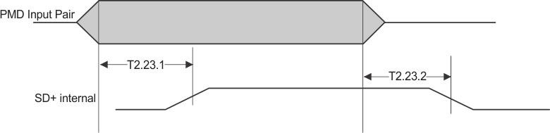 Figure 23. 100BASE-TX Signal Detect Timing
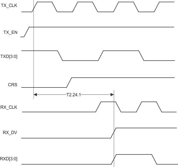 Figure 24. 100 Mb/s Internal Loopback Timing
 Figure 25. 10 Mb/s Internal Loopback Timing
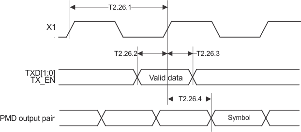 Figure 26. RMII Transmit Timing
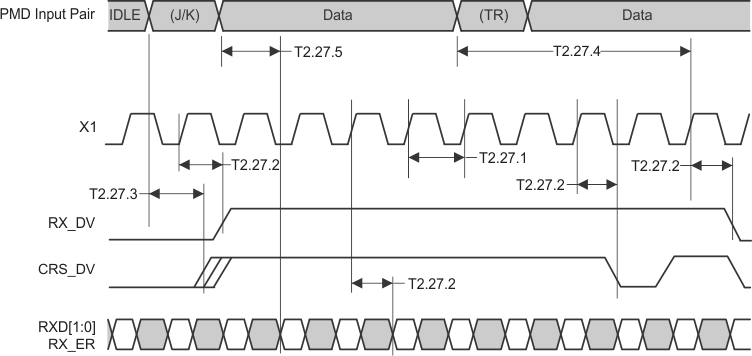 Figure 27. RMII Receive Timing
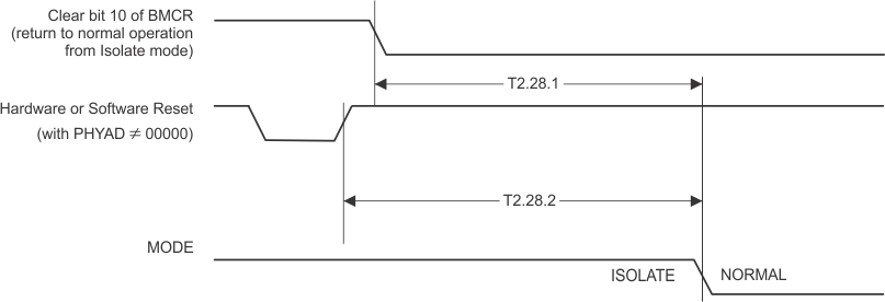 Figure 28. Isolation Timing
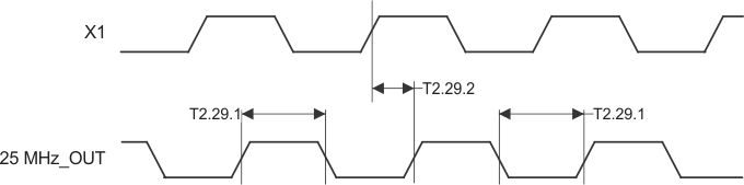 Figure 29. 25 MHz_OUT Timing