SBVS206A November 2012 – March 2015 DRV10866
PRODUCTION DATA.
- 1 Features
- 2 Applications
- 3 Description
- 4 Revision History
- 5 Pin Configuration and Functions
- 6 Specifications
- 7 Detailed Description
- 8 Application and Implementation
- 9 Power Supply Recommendations
- 10Layout
- 11Device and Documentation Support
- 12Mechanical, Packaging, and Orderable Information
Package Options
Mechanical Data (Package|Pins)
- DSC|10
Thermal pad, mechanical data (Package|Pins)
- DSC|10
Orderable Information
10 Layout
10.1 Layout Guidelines
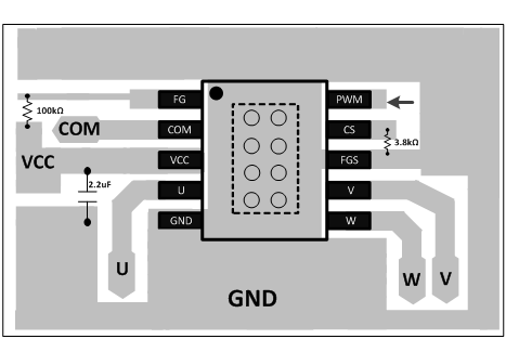
The DRV10866 is simple to design with a single-layer or two layer printed-circuit-board (PCB) layout. During layout, the strategy of ground copper pour is very important to enhance the thermal performance. Use vias on the thermal pad to dissipate heat away from the IC. Refer to Figure 18 for an example of PCB layout.
- Place VCC, GND, U, V, and W pins with thick traces because high current passes through these traces.
- Place the 2.2-μF capacitor between VCC and GND, and as close to the VCC and GND pins as possible.
- Connect the GND under the thermal pad.
- Keep the thermal pad connection as large as possible, both on the bottom side and top side. It should be one piece of copper without any gaps.
10.2 Layout Example
 Figure 18. PCB Layout Example