SBVS206A November 2012 – March 2015 DRV10866
PRODUCTION DATA.
- 1 Features
- 2 Applications
- 3 Description
- 4 Revision History
- 5 Pin Configuration and Functions
- 6 Specifications
- 7 Detailed Description
- 8 Application and Implementation
- 9 Power Supply Recommendations
- 10Layout
- 11Device and Documentation Support
- 12Mechanical, Packaging, and Orderable Information
Package Options
Mechanical Data (Package|Pins)
- DSC|10
Thermal pad, mechanical data (Package|Pins)
- DSC|10
Orderable Information
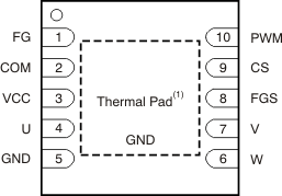
5 Pin Configuration and Functions
10-Pins WSON with Thermal Pad
DSC Package
Top View

(1) Thermal pad connected to ground.
Pin Functions
| PIN | I/O | DESCRIPTION | |
|---|---|---|---|
| NAME | NO. | ||
| COM | 2 | I | Motor common terminal input |
| CS | 9 | I | Overcurrent threshold setup pin. The constant current of the internal constant current source flows through the resistor connected to this pin. The other side of the resistor is connected to ground. The voltage across the resistor compares with the voltage converted from the bottom MOSFET current. If the MOSFET current is high, the part enters the overcurrent protection mode by turning off the top PWM MOSFET and holding the bottom MOSFET on. I (mA) = 3120/RCS(kΩ). Equation valid range: 300 mA < ILIMIT< 850 mA |
| FG | 1 | O | Frequency generator output. If the FGS pin is connected to ground, the output has a period equal to one electrical cycle (FG). If the FGS pin is connected to VCC, the output has a period equal to two electrical cycles (1/2FG). |
| FGS | 8 | I | FG and 1/2FG control pin. Latched upon wake-up signal from the PWM pin. For details, refer to Frequency Generator. |
| GND | 5 | — | Ground pin |
| PWM | 10 | I | PWM input pin. The PWM input signal is converted to a fixed 156-kHz switching frequency on the MOSFET driver. The PWM input signal resolution is less than 1%. This pin can also control the device and put it in or out of standby mode. After the signal at the PWM stays low (up to 500 µs), the device goes into low-power standby mode. Standby current is approximately 5 µA. The rising edge of the PWM signal wakes up the device and puts it into active mode, where it is ready to start to turn the motor. |
| U | 4 | O | Phase U output |
| V | 7 | O | Phase V output |
| VCC | 3 | I | Input voltage for motor and chip-supply voltage; the internal clamping circuit clamps the VCC voltage. |
| W | 6 | O | Phase W output |