SLVSF30A October 2019 – October 2021 DRV10982-Q1
PRODUCTION DATA
- 1 Features
- 2 Applications
- 3 Description
- 4 Revision History
- 5 Description (Continued)
- 6 Pin Configuration and Functions
- 7 Specifications
-
8 Detailed Description
- 8.1 Overview
- 8.2 Functional Block Diagram
- 8.3 Feature Description
- 8.4
Device Functional Modes
- 8.4.1 Motor Parameters
- 8.4.2 Starting the Motor Under Different Initial Conditions
- 8.4.3 Motor Start Sequence
- 8.4.4 Align Current
- 8.4.5 Start-Up Current Setting
- 8.4.6 Closed Loop
- 8.4.7 Current Limit
- 8.4.8 Lock Detect and Fault Handling
- 8.4.9 Anti Voltage Suppression Function
- 8.4.10 PWM Output
- 8.4.11 FG Customized Configuration
- 8.4.12
Diagnostics and Visibility
- 8.4.12.1 Motor-Status Readback
- 8.4.12.2 Motor-Speed Readback
- 8.4.12.3 Motor Electrical-Period Readback
- 8.4.12.4 BEMF Constant Read Back
- 8.4.12.5 Motor Estimated Position by IPD
- 8.4.12.6 Supply-Voltage Readback
- 8.4.12.7 Speed-Command Readback
- 8.4.12.8 Speed-Command Buffer Readback
- 8.4.12.9 Fault Diagnostics
- 8.5
Register Maps
- 8.5.1 I2C Serial Interface
- 8.5.2 Register Map
- 8.5.3
Register Descriptions
- 8.5.3.1 FaultReg Register (address = 0x00) [reset = 0x00]
- 8.5.3.2 MotorSpeed Register (address = 0x01) [reset = 0x00]
- 8.5.3.3 MotorPeriod Register (address = 0x02) [reset = 0x00]
- 8.5.3.4 MotorKt Register (address = 0x03) [reset = 0x00]
- 8.5.3.5 MotorCurrent Register (address = 0x04) [reset = 0x00]
- 8.5.3.6 IPDPosition–SupplyVoltage Register (address = 0x05) [reset = 0x00]
- 8.5.3.7 SpeedCmd–spdCmdBuffer Register (address = 0x06) [reset = 0x00]
- 8.5.3.8 AnalogInLvl Register (address = 0x07) [reset = 0x00]
- 8.5.3.9 DeviceID–RevisionID Register (address = 0x08) [reset = 0x00]
- 8.5.3.10 DeviceID–RevisionID Register (address = 0x08) [reset = 0x00]
- 8.5.3.11 Unused Registers (addresses = 0x011 Through 0x2F)
- 8.5.3.12 SpeedCtrl Register (address = 0x30) [reset = 0x00]
- 8.5.3.13 EEPROM Programming1 Register (address = 0x31) [reset = 0x00]
- 8.5.3.14 EEPROM Programming2 Register (address = 0x32) [reset = 0x00]
- 8.5.3.15 EEPROM Programming3 Register (address = 0x33) [reset = 0x00]
- 8.5.3.16 EEPROM Programming4 Register (address = 0x34) [reset = 0x00]
- 8.5.3.17 EEPROM Programming5 Register (address = 0x35) [reset = 0x00]
- 8.5.3.18 EEPROM Programming6 Register (address = 0x36) [reset = 0x00]
- 8.5.3.19 Unused Registers (addresses = 0x37 Through 0x5F)
- 8.5.3.20 EECTRL Register (address = 0x60) [reset = 0x00]
- 8.5.3.21 Unused Registers (addresses = 0x61 Through 0x8F)
- 8.5.3.22 CONFIG1 Register (address = 0x90) [reset = 0x00]
- 8.5.3.23 CONFIG2 Register (address = 0x91) [reset = 0x00]
- 8.5.3.24 CONFIG3 Register (address = 0x92) [reset = 0x00]
- 8.5.3.25 CONFIG4 Register (address = 0x93) [reset = 0x00]
- 8.5.3.26 CONFIG5 Register (address = 0x94) [reset = 0x00]
- 8.5.3.27 CONFIG6 Register (address = 0x95) [reset = 0x00]
- 8.5.3.28 CONFIG7 Register (address = 0x96) [reset = 0x00]
- 9 Application and Implementation
- 10Power Supply Recommendations
- 11Layout
- 12Device and Documentation Support
- 13Mechanical, Packaging, and Orderable Information
Package Options
Mechanical Data (Package|Pins)
- PWP|24
Thermal pad, mechanical data (Package|Pins)
- PWP|24
Orderable Information
7.5 Electrical Characteristics
over operating voltage and ambient temperature range (unless otherwise noted)
| PARAMETER | TEST CONDITIONS | MIN | TYP | MAX | UNIT | |
|---|---|---|---|---|---|---|
| SUPPLY CURRENT (DRV10982Q) | ||||||
| IVccSLEEP1 | Sleep current | VSPEED = 0 V; VCC = 12 V; TA = 25℃ | 48 | 54 | µA | |
| VSPEED = 0 V; VCC = 12 V; across temperature | 81 | |||||
| IVcc | Active current | VSPEED > 0 V; buck regulator with inductor; no motor load | 10 | 15 | mA | |
| VSPEED > 0 V; buck regulator with resistor; no motor load | 13 | 16 | ||||
| SUPPLY CURRENT (DRV10982SQ) | ||||||
| IVccSTBY | Standby current | VSPEED = 0 V; buck regulator with inductor | 8.5 | 14 | mA | |
| VSPEED = 0 V; buck regulator with resistor | 11 | 15 | ||||
| IVcc | Active current | VSPEED > 0 V; buck regulator with inductor; no motor load | 10 | 15 | mA | |
| VSPEED > 0 V; buck regulator with resistor; no motor load | 13 | 16 | ||||
| UVLO | ||||||
| VUVLO_R | UVLO rising threshold voltage | 5.8 | 6 | 6.2 | V | |
| VUVLO_F | UVLO falling threshold voltage | 5.6 | 5.8 | 6 | V | |
| VUVLO_HYS | UVLO threshold voltage hysteresis | 170 | 195 | 220 | mV | |
| VV1P8_UVLO_R | V1P8 UVLO rising threshold | 1.5 | 1.6 | 1.7 | V | |
| VV1P8_UVLO_F | V1P8 UVLO falling threshold | 1.4 | 1.55 | 1.65 | V | |
| VV3P3_UVLO_R | V3P3 UVLO rising threshold | 2.7 | 2.85 | 2.95 | V | |
| VV3P3_UVLO_F | V3P3 UVLO falling threshold | 2.5 | 2.7 | 2.8 | V | |
| VVREG_UVLO_R | VREG UVLO rising threshold | 4 | 4.2 | 4.3 | V | |
| VVREG_UVLO_F | VREG UVLO falling threshold | 3.9 | 4.2 | V | ||
| LDO OUTPUT | ||||||
| V3P3 | Output voltage | Buck regulator with inductor, 20-mA load | 3.1 | 3.3 | 3.5 | V |
| Buck regulator with resistor, no load | ||||||
| IV3P3_MAX | Maximum load from V3P3 | Only with inductor mode of buck operation, with resistor mode no load | 20 | mA | ||
| V1P8 | Output voltage | No load | 1.7 | 1.8 | 1.9 | V |
| STEP-DOWN REGULATOR | ||||||
| VREG | Regulator output voltage | LSW = 47 µH, CSW = 10 µF Iload = 100 mA | 4.5 | 5 | 5.5 | V |
| RSW = 39 Ω, CSW = 10 µF Iload = 5 mA | ||||||
| IREG_MAX_L | Maximum load from VREG in switching mode | LSW = 47 µH, CSW = 10 µF | 100 | mA | ||
| IREG_MAX_R | Maximum load from VREG in linear mode | RSW = 39 Ω, CSW = 10 µF | 5 | mA | ||
| INTEGRATED MOSFET | ||||||
| rDS(ON) | Series resistance (H + L) | TA = 25°C; V(VCC) > 6.5 V; Io = 1 A | 300 | 400 | mΩ | |
| TA = 125°C; V(VCC) > 6.5V; Io = 1 A | 400 | 550 | ||||
| SPEED – ANALOG MODE | ||||||
| VAN/A_FS | Analog full-speed voltage | V(V3P3) × 0.9 | V(V3P3) | V | ||
| VAN/A_ZS | Analog zero-speed voltage | 0 | 100 | mV | ||
| tSAM | Sampling period for analog voltage on SPEED pin | 320 | µs | |||
| VAN/A_RES | Analog voltage resolution | 6.5 | mV | |||
| SPEED – PWM DIGITAL MODE | ||||||
| VDIG_IH | PWM input high voltage | 2.2 | V | |||
| VDIG_IL | PWM input low voltage | 0.6 | V | |||
| ƒPWM | PWM input frequency | 0.1 | 100 | kHz | ||
| STANDBY MODE (DRV10982SQ) | ||||||
| VEN_SB | Analog voltage to enter standby mode | SpdCtrlMd = 0 (analog mode) | 100 | mV | ||
| VEX_SB | Analog voltage to exit standby mode | SpdCtrlMd = 0 (analog mode) | 0.17 | V | ||
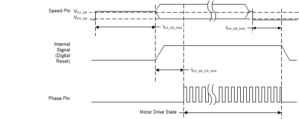
| tEX_SB_ANA | Time needed to exit from standby mode | SpdCtrlMd = 0 (analog mode) VSPEED > VEX_SB | 1 | 700 | ms | |
| tEX_SB_DR_ANA | Time taken to drive motor after exiting standby mode | SpdCtrlMd = 0 (analog mode) VSPEED > VEX_SB; ISDen = 0; BrkDoneThr[2:0] = 0 | 350 | ms | ||
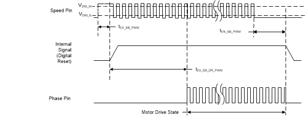
| tEX_SB_PWM | Time needed to exit from standby mode | SpdCtrlMd = 1 (PWM mode) VSPEED > VDIG_IH | 2 | µs | ||
| tEX_SB_DR_PWM | Time taken to drive motor after exiting standby mode | SpdCtrlMd = 1 (PWM mode) VSPEED_DUTY > 0; ISDen = 0; BrkDoneThr[2:0] = 0 | 350 | ms | ||
| tEN_SB_ANA | Time needed to enter standby mode | SpdCtrlMd = 0 (analog mode) VSPEED < VEN_SB; AvSIndEn = 0 | 6 | ms | ||
| tEN_SB_PWM | Time needed to enter standby mode | SpdCtrlMd = 1 (PMW mode) VSPEED < VDIG_IL; AvSIndEn = 0 | 60 | ms | ||
| SLEEP MODE (DRV10982Q) | ||||||
| VEN_SL | Analog voltage to enter sleep mode | SpdCtrlMd = 0 (analog mode) | 100 | mV | ||
| VEX_SL | Analog voltage to exit sleep mode | SpdCtrlMd = 0 (analog mode) | 2.2 | V | ||
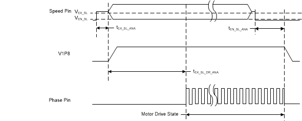
| tEX_SL_ANA | Time needed to exit from sleep mode | SpdCtrlMd = 0 (analog mode) VSPEED > VEX_SL | 2 | µs | ||
| tEX_SL_DR_ANA | Time taken to drive motor after exiting from sleep mode | SpdCtrlMd = 0 (analog mode) VSPEED > VEX_SL; ISDen = 0; BrkDoneThr[2:0] = 0 | 350 | ms | ||
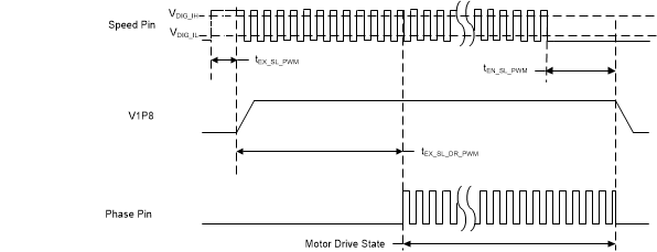
| tEX_SL_PWM | Time needed to exit from sleep mode | SpdCtrlMd = 1 (PWM mode) VSPEED > VDIG_IH | 2 | µs | ||
| tEX_SL_DR_PWM | Time taken to drive motor after exiting from sleep mode | SpdCtrlMd = 1 (PWM mode) VSPEED > VDIG_IH; ISDen = 0; BrkDoneThr[2:0] = 0 | 350 | ms | ||
| tEN_SL_ANA | Time needed to enter sleep mode | SpdCtrlMd = 0 (analog mode) VSPEED < VEN_SL; AvSIndEn = 0 | 6 | ms | ||
| tEN_SL_PWM | Time needed to enter sleep mode | SpdCtrlMd = 1 (PMW mode) VSPEED < VDIG_IL; AvSIndEn = 0 | 60 | ms | ||
| RPD_SPEED_SL | Internal SPEED pin pull down resistance to ground | VSPEED = 0 (Sleep mode) | 55 | kΩ | ||
| DIGITAL I/O (DIR INPUT, FG OUTPUT ) | ||||||
| VDIR_H | Input high | 2.2 | V | |||
| VDIR_L | Input low | 0.6 | V | |||
| VFG_OH | Output high voltage Io = 5 mA | 3.3 | V | |||
| VFG_OL | Output low voltage Io = 5 mA | 0.6 | V | |||
| I2C SERIAL INTERFACE | ||||||
| VI2C_H | Input high | 2.2 | V | |||
| VI2C_L | Input low | 0.6 | V | |||
| fI2C | I2C clock frequency | 0 | 400 | kHz | ||
| LOCK DETECTION RELEASE TIME | ||||||
| tLOCK_OFF | Lock release time | 5 | s | |||
| tLCK_ETR | Lock enter time | 0.3 | s | |||
| OVERCURRENT PROTECTION | ||||||
| IOC_limit_HS | HS overcurrent protection | VCC < 28.5 V | 3.5 | 4.25 | 5.5 | A |
| IOC_limit_LS | LS overcurrent protection | VCC < 28.5 V | 3.5 | 4.25 | 5.5 | A |
| THERMAL SHUTDOWN | ||||||
| TSDN | Junction temperature shutdown threshold | 150 | 165 | 180 | °C | |
| TSDN_HYS | Junction temperature shutdown hysteresis | 15 | 20 | 25 | °C | |
| TWARN | Junction temperature warning threshold | 115 | 125 | 140 | °C | |
| PHASE DRIVER | ||||||
| SLPH_LH0 | Phase slew rate switching low to high | PHslew = 0; measure 20% to 80%; VCC = 12 V | 85 | 120 | 145 | V/µs |
| SLPH_LH1 | Phase slew rate switching low to high | PHslew = 1; measure 20% to 80%; VCC = 12 V | 60 | 80 | 100 | V/µs |
| SLPH_LH2 | Phase slew rate switching low to high | PHslew = 2; measure 20% to 80%; VCC = 12 V | 38 | 50 | 62 | V/µs |
| SLPH_LH3 | Phase slew rate switching low to high | PHslew = 3; measure 20% to 80%; VCC = 12 V | 27 | 35 | 44 | V/µs |
| SLPH_HL0 | Phase slew rate switching high to low | PHslew = 0; measure 80% to 20%; VCC = 12 V | 85 | 120 | 145 | V/µs |
| SLPH_HL1 | Phase slew rate switching high to low | PHslew = 1; measure 80% to 20%; VCC = 12 V | 59 | 80 | 100 | V/µs |
| SLPH_HL2 | Phase slew rate switching high to low | PHslew = 2; measure 80% to 20%; VCC = 12 V | 36 | 50 | 60 | V/µs |
| SLPH_HL3 | Phase slew rate switching high to low | PHslew = 3; measure 80% to 20%; VCC = 12 V | 25 | 35 | 45 | V/µs |
| BEMF COMPARATOR | ||||||
| BEMFHYS | BEMF comparator hysteresis | BEMF_HYS = 0 | 7 | 20 | 30 | mV |
| BEMF_HYS = 1 | 17 | 40 | 51 | |||
| LOAD DUMP PROTECTION | ||||||
| VOV_R | Load dump protection mode entry on rising VCC threshold | 28.5 | 29.2 | 30 | V | |
| VOV_F | Load dump protection mode exit on falling VCC threshold | 27.7 | 28.2 | 28.8 | V | |
| VOV_HYS | Load dump protection mode hysteresis | 0.73 | 1 | 1.1 | V | |
 Figure 7-1 DRV10982Q Analog Mode Timing
 Figure 7-2 DRV10982Q PWM Mode Timing
 Figure 7-3 DRV10982SQ Analog Mode Timing
 Figure 7-4 DRV10982SQ PWM Mode Timing