SLVSF30A October 2019 – October 2021 DRV10982-Q1
PRODUCTION DATA
- 1 Features
- 2 Applications
- 3 Description
- 4 Revision History
- 5 Description (Continued)
- 6 Pin Configuration and Functions
- 7 Specifications
-
8 Detailed Description
- 8.1 Overview
- 8.2 Functional Block Diagram
- 8.3 Feature Description
- 8.4
Device Functional Modes
- 8.4.1 Motor Parameters
- 8.4.2 Starting the Motor Under Different Initial Conditions
- 8.4.3 Motor Start Sequence
- 8.4.4 Align Current
- 8.4.5 Start-Up Current Setting
- 8.4.6 Closed Loop
- 8.4.7 Current Limit
- 8.4.8 Lock Detect and Fault Handling
- 8.4.9 Anti Voltage Suppression Function
- 8.4.10 PWM Output
- 8.4.11 FG Customized Configuration
- 8.4.12
Diagnostics and Visibility
- 8.4.12.1 Motor-Status Readback
- 8.4.12.2 Motor-Speed Readback
- 8.4.12.3 Motor Electrical-Period Readback
- 8.4.12.4 BEMF Constant Read Back
- 8.4.12.5 Motor Estimated Position by IPD
- 8.4.12.6 Supply-Voltage Readback
- 8.4.12.7 Speed-Command Readback
- 8.4.12.8 Speed-Command Buffer Readback
- 8.4.12.9 Fault Diagnostics
- 8.5
Register Maps
- 8.5.1 I2C Serial Interface
- 8.5.2 Register Map
- 8.5.3
Register Descriptions
- 8.5.3.1 FaultReg Register (address = 0x00) [reset = 0x00]
- 8.5.3.2 MotorSpeed Register (address = 0x01) [reset = 0x00]
- 8.5.3.3 MotorPeriod Register (address = 0x02) [reset = 0x00]
- 8.5.3.4 MotorKt Register (address = 0x03) [reset = 0x00]
- 8.5.3.5 MotorCurrent Register (address = 0x04) [reset = 0x00]
- 8.5.3.6 IPDPosition–SupplyVoltage Register (address = 0x05) [reset = 0x00]
- 8.5.3.7 SpeedCmd–spdCmdBuffer Register (address = 0x06) [reset = 0x00]
- 8.5.3.8 AnalogInLvl Register (address = 0x07) [reset = 0x00]
- 8.5.3.9 DeviceID–RevisionID Register (address = 0x08) [reset = 0x00]
- 8.5.3.10 DeviceID–RevisionID Register (address = 0x08) [reset = 0x00]
- 8.5.3.11 Unused Registers (addresses = 0x011 Through 0x2F)
- 8.5.3.12 SpeedCtrl Register (address = 0x30) [reset = 0x00]
- 8.5.3.13 EEPROM Programming1 Register (address = 0x31) [reset = 0x00]
- 8.5.3.14 EEPROM Programming2 Register (address = 0x32) [reset = 0x00]
- 8.5.3.15 EEPROM Programming3 Register (address = 0x33) [reset = 0x00]
- 8.5.3.16 EEPROM Programming4 Register (address = 0x34) [reset = 0x00]
- 8.5.3.17 EEPROM Programming5 Register (address = 0x35) [reset = 0x00]
- 8.5.3.18 EEPROM Programming6 Register (address = 0x36) [reset = 0x00]
- 8.5.3.19 Unused Registers (addresses = 0x37 Through 0x5F)
- 8.5.3.20 EECTRL Register (address = 0x60) [reset = 0x00]
- 8.5.3.21 Unused Registers (addresses = 0x61 Through 0x8F)
- 8.5.3.22 CONFIG1 Register (address = 0x90) [reset = 0x00]
- 8.5.3.23 CONFIG2 Register (address = 0x91) [reset = 0x00]
- 8.5.3.24 CONFIG3 Register (address = 0x92) [reset = 0x00]
- 8.5.3.25 CONFIG4 Register (address = 0x93) [reset = 0x00]
- 8.5.3.26 CONFIG5 Register (address = 0x94) [reset = 0x00]
- 8.5.3.27 CONFIG6 Register (address = 0x95) [reset = 0x00]
- 8.5.3.28 CONFIG7 Register (address = 0x96) [reset = 0x00]
- 9 Application and Implementation
- 10Power Supply Recommendations
- 11Layout
- 12Device and Documentation Support
- 13Mechanical, Packaging, and Orderable Information
Package Options
Mechanical Data (Package|Pins)
- PWP|24
Thermal pad, mechanical data (Package|Pins)
- PWP|24
Orderable Information
8.4.11.1 FG Output Frequency
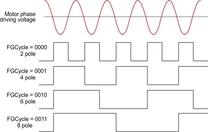
The FG output frequency can be configured by FGcycle[3:0]. The default FG toggles once every electrical cycle (FGcycle = 0000). Many applications configure the FG output so that it provides two pulses for every mechanical rotation of the motor. The configuration bits provided in the DRV10982-Q1 device can accomplish this for 2-pole, 4-pole, 6-pole, and 8-pole motors up to 32-pole motors. This is illustrated in Figure 8-36 for 2, 4, 6, and 8-pole motors.
Figure 8-36 shows the DRV10982-Q1 device has been configured to provide FG pulses once every electrical cycle (4 poles), twice every three electrical cycles (6 poles), once every two electrical cycles (8 poles), and once every three electrical cycles (12 poles).
Note that when it is set to two FG pulses every three electrical cycles, the FG output is not 50% duty cycle. Motor speed is able to be measured by monitoring the rising edge of the FG output.
 Figure 8-36 FG Frequency Divider