SLVSF30A October 2019 – October 2021 DRV10982-Q1
PRODUCTION DATA
- 1 Features
- 2 Applications
- 3 Description
- 4 Revision History
- 5 Description (Continued)
- 6 Pin Configuration and Functions
- 7 Specifications
-
8 Detailed Description
- 8.1 Overview
- 8.2 Functional Block Diagram
- 8.3 Feature Description
- 8.4
Device Functional Modes
- 8.4.1 Motor Parameters
- 8.4.2 Starting the Motor Under Different Initial Conditions
- 8.4.3 Motor Start Sequence
- 8.4.4 Align Current
- 8.4.5 Start-Up Current Setting
- 8.4.6 Closed Loop
- 8.4.7 Current Limit
- 8.4.8 Lock Detect and Fault Handling
- 8.4.9 Anti Voltage Suppression Function
- 8.4.10 PWM Output
- 8.4.11 FG Customized Configuration
- 8.4.12
Diagnostics and Visibility
- 8.4.12.1 Motor-Status Readback
- 8.4.12.2 Motor-Speed Readback
- 8.4.12.3 Motor Electrical-Period Readback
- 8.4.12.4 BEMF Constant Read Back
- 8.4.12.5 Motor Estimated Position by IPD
- 8.4.12.6 Supply-Voltage Readback
- 8.4.12.7 Speed-Command Readback
- 8.4.12.8 Speed-Command Buffer Readback
- 8.4.12.9 Fault Diagnostics
- 8.5
Register Maps
- 8.5.1 I2C Serial Interface
- 8.5.2 Register Map
- 8.5.3
Register Descriptions
- 8.5.3.1 FaultReg Register (address = 0x00) [reset = 0x00]
- 8.5.3.2 MotorSpeed Register (address = 0x01) [reset = 0x00]
- 8.5.3.3 MotorPeriod Register (address = 0x02) [reset = 0x00]
- 8.5.3.4 MotorKt Register (address = 0x03) [reset = 0x00]
- 8.5.3.5 MotorCurrent Register (address = 0x04) [reset = 0x00]
- 8.5.3.6 IPDPosition–SupplyVoltage Register (address = 0x05) [reset = 0x00]
- 8.5.3.7 SpeedCmd–spdCmdBuffer Register (address = 0x06) [reset = 0x00]
- 8.5.3.8 AnalogInLvl Register (address = 0x07) [reset = 0x00]
- 8.5.3.9 DeviceID–RevisionID Register (address = 0x08) [reset = 0x00]
- 8.5.3.10 DeviceID–RevisionID Register (address = 0x08) [reset = 0x00]
- 8.5.3.11 Unused Registers (addresses = 0x011 Through 0x2F)
- 8.5.3.12 SpeedCtrl Register (address = 0x30) [reset = 0x00]
- 8.5.3.13 EEPROM Programming1 Register (address = 0x31) [reset = 0x00]
- 8.5.3.14 EEPROM Programming2 Register (address = 0x32) [reset = 0x00]
- 8.5.3.15 EEPROM Programming3 Register (address = 0x33) [reset = 0x00]
- 8.5.3.16 EEPROM Programming4 Register (address = 0x34) [reset = 0x00]
- 8.5.3.17 EEPROM Programming5 Register (address = 0x35) [reset = 0x00]
- 8.5.3.18 EEPROM Programming6 Register (address = 0x36) [reset = 0x00]
- 8.5.3.19 Unused Registers (addresses = 0x37 Through 0x5F)
- 8.5.3.20 EECTRL Register (address = 0x60) [reset = 0x00]
- 8.5.3.21 Unused Registers (addresses = 0x61 Through 0x8F)
- 8.5.3.22 CONFIG1 Register (address = 0x90) [reset = 0x00]
- 8.5.3.23 CONFIG2 Register (address = 0x91) [reset = 0x00]
- 8.5.3.24 CONFIG3 Register (address = 0x92) [reset = 0x00]
- 8.5.3.25 CONFIG4 Register (address = 0x93) [reset = 0x00]
- 8.5.3.26 CONFIG5 Register (address = 0x94) [reset = 0x00]
- 8.5.3.27 CONFIG6 Register (address = 0x95) [reset = 0x00]
- 8.5.3.28 CONFIG7 Register (address = 0x96) [reset = 0x00]
- 9 Application and Implementation
- 10Power Supply Recommendations
- 11Layout
- 12Device and Documentation Support
- 13Mechanical, Packaging, and Orderable Information
Package Options
Mechanical Data (Package|Pins)
- PWP|24
Thermal pad, mechanical data (Package|Pins)
- PWP|24
Orderable Information
8.4.1.1 Motor Phase Resistance
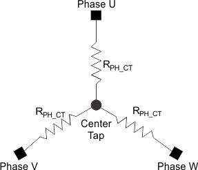
For a wye-connected motor, the motor phase resistance refers to the resistance from the phase output to the center tap, RPH_CT (denoted as RPH_CT in Figure 8-7).
 Figure 8-7 Wye-Connected Motor Phase Resistance
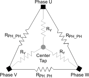
For a delta-connected motor, the motor phase resistance refers to the equivalent phase to center tap in the wye configuration. In Figure 8-8, it is denoted as RY. RPH_CT = RY.
For both the delta-connected motor and the wye-connected motor, the easy way to get the equivalent RPH_CT is to measure the resistance between two phase terminals (RPH_PH), and then divide this value by two, RPH_CT = ½ RPH_PH.
 Figure 8-8 Delta-Connected Motor and the Equivalent Wye Connections
The motor phase resistance (RPH_CT) must be converted to a 7-bit digital register value Rm[6:0] to program the motor phase resistance value. The digital register value can be determined as follows:
- Convert the motor phase resistance (RPH_CT) to a digital value where the LSB is weighted to represent 9.67 mΩ: Rmdig = RPH_CT / 0.00967.
- Encode the digital value such that Rmdig = RMValue[3:0] << RMShift[2:0].
The maximum resistor value, RPH_CT, that can be programmed for the DRV10982-Q1 device is 18.5 Ω, which represents Rmdig = 1920 and an encoded Rm[6:0] value of 0x7Fh. The minimum resistor the DRV10982-Q1 device supports is 0.029 Ω, RPH_CT, which represents Rmdig = 3.
For convenience, the encoded value for Rm[6:0] can also be obtained from Table 8-3.
| RM[6:0] {RMShift[2:0], RMValue[3:0]} | RPH_CT (Ω) | RM[6:0] {RMShift[2:0], RMValue[3:0]} | RPH_CT (Ω) | RM[6:0] {RMShift[2:0], RMValue[3:0]} | RPH_CT (Ω) | |||||
|---|---|---|---|---|---|---|---|---|---|---|
| BINARY | HEX | BINARY | HEX | BINARY | HEX | |||||
| 000 0000 | 0x00 | 0 | 0101000 | 0x28 | 0.3104 | 1011000 | 0x58 | 2.4832 | ||
| 000 0001 | 0x01 | 0.0097 | 010 1001 | 0x29 | 0.3492 | 101 1001 | 0x59 | 2.7936 | ||
| 000 0010 | 0x02 | 0.0194 | 010 1010 | 0x2A | 0.388 | 101 1010 | 0x5A | 3.104 | ||
| 000 0011 | 0x03 | 0.0291 | 010 1011 | 0x2B | 0.4268 | 101 1011 | 0x5B | 3.4144 | ||
| 000 0100 | 0x04 | 0.0388 | 010 1100 | 0x2C | 0.4656 | 101 1100 | 0x5C | 3.7248 | ||
| 000 0101 | 0x05 | 0.0485 | 010 1101 | 0x2D | 0.5044 | 101 1101 | 0x5D | 4.0352 | ||
| 000 0110 | 0x06 | 0.0582 | 010 1110 | 0x2E | 0.5432 | 101 1110 | 0x5E | 4.3456 | ||
| 000 0111 | 0x07 | 0.0679 | 010 1111 | 0x2F | 0.582 | 101 1111 | 0x5F | 4.656 | ||
| 000 1000 | 0x08 | 0.0776 | 011 1000 | 0x38 | 0.6208 | 110 1000 | 0x68 | 4.9664 | ||
| 000 1001 | 0x09 | 0.0873 | 011 1001 | 0x39 | 0.6984 | 110 1001 | 0x69 | 5.5872 | ||
| 000 1010 | 0x0A | 0.097 | 011 1010 | 0x3A | 0.776 | 110 1010 | 0x6A | 6.208 | ||
| 000 1011 | 0x0B | 0.1067 | 011 1011 | 0x3B | 0.8536 | 110 1011 | 0x6B | 6.8288 | ||
| 000 1100 | 0x0C | 0.1164 | 011 1100 | 0x3C | 0.9312 | 110 1100 | 0x6C | 7.4496 | ||
| 000 1101 | 0x0D | 0.1261 | 011 1101 | 0x3D | 1.0088 | 110 1101 | 0x6D | 8.0704 | ||
| 000 1110 | 0x0E | 0.1358 | 011 1110 | 0x3E | 1.0864 | 110 1110 | 0x6E | 8.6912 | ||
| 000 1111 | 0x0F | 0.1455 | 011 1111 | 0x3F | 1.164 | 110 1111 | 0x6F | 9.312 | ||
| 001 1000 | 0x18 | 0.1552 | 100 1000 | 0x48 | 1.2416 | 111 1000 | 0x78 | 9.9328 | ||
| 001 1001 | 0x19 | 0.1746 | 100 1001 | 0x49 | 1.3968 | 111 1001 | 0x79 | 11.1744 | ||
| 001 1010 | 0x1A | 0.194 | 100 1010 | 0x4A | 1.552 | 111 1010 | 0x7A | 12.416 | ||
| 001 1011 | 0x1B | 0.2134 | 100 1011 | 0x4B | 1.7072 | 111 1011 | 0x7B | 13.6576 | ||
| 001 1100 | 0x1C | 0.2328 | 100 1100 | 0x4C | 1.8624 | 111 1100 | 0x7C | 14.8992 | ||
| 001 1101 | 0x1D | 0.2522 | 100 1101 | 0x4D | 2.0176 | 111 1101 | 0x7D | 16.1408 | ||
| 001 1110 | 0x1E | 0.2716 | 100 1110 | 0x4E | 2.1728 | 111 1110 | 0x7E | 17.3824 | ||
| 001 1111 | 0x1F | 0.291 | 100 1111 | 0x4F | 2.328 | 111 1111 | 0x7F | 18.624 | ||