SLVSBA8G March   2012  – March 2018 DRV110

PRODUCTION DATA.  

  1. Features
  2. Applications
  3. Description
    1.     Device Images
      1.      DRV110 Supplied by Power Line Voltage
  4. Revision History
  5. Pin Configuration and Functions
    1.     Pin Functions
  6. Specifications
    1. 6.1 Absolute Maximum Ratings
    2. 6.2 ESD Ratings
    3. 6.3 Recommended Operating Conditions
    4. 6.4 Thermal Information
    5. 6.5 Electrical Characteristics
    6. 6.6 Typical Characteristics
  7. Detailed Description
    1. 7.1 Overview
    2. 7.2 Functional Block Diagram
    3. 7.3 Feature Description
      1. 7.3.1 Keep Time
      2. 7.3.2 PWM Current Control
      3. 7.3.3 Configuring Peak and Hold Currents
      4. 7.3.4 Configuring the PWM Frequency
      5. 7.3.5 Voltage Supply and Integrated Zener Diode
    4. 7.4 Device Functional Modes
      1. 7.4.1 Normal Mode
      2. 7.4.2 Shutdown
  8. Application and Implementation
    1. 8.1 Application Information
    2. 8.2 Typical Application
      1. 8.2.1 Design Requirements
      2. 8.2.2 Detailed Design Procedure
        1. 8.2.2.1 Current Limiting Resistor Selection
        2. 8.2.2.2 Passive Component Selection
      3. 8.2.3 Application Curve
  9. Power Supply Recommendations
  10. 10Layout
    1. 10.1 Layout Guidelines
    2. 10.2 Layout Example
  11. 11Device and Documentation Support
    1. 11.1 Documentation Support
      1. 11.1.1 Related Documentation
    2. 11.2 Receiving Notification of Documentation Updates
    3. 11.3 Community Resources
    4. 11.4 Trademarks
    5. 11.5 Electrostatic Discharge Caution
    6. 11.6 Glossary
  12. 12Mechanical, Packaging, and Orderable Information

Package Options

Mechanical Data (Package|Pins)
Thermal pad, mechanical data (Package|Pins)
Orderable Information

Configuring the PWM Frequency

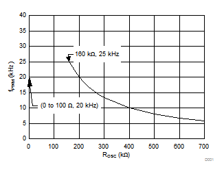
Frequency of the internal PWM clock signal, PWMCLK, that triggers each OUT pin ON-cycle can be adjusted by external resistor, ROSC, connected between OSC and GND. Frequency as a function of resistor value is shown in Figure 5. Default frequency is used when OSC is connected to GND directly. Use Equation 4 to calculate the PWM frequency as a function of the external fixed adjustment resistor value (greater than 160 kΩ).

Equation 4. DRV110 eq4_lvsba8.gif
DRV110 pwm_clock_lvsba8.gifFigure 5. PWM Clock Frequency Setting