SLWS237A November 2012 – November 2014 DRV11873
PRODUCTION DATA.
- 1 Features
- 2 Applications
- 3 Description
- 4 Simplified Schematic
- 5 Revision History
- 6 Pin Configuration and Functions
- 7 Specifications
- 8 Detailed Description
- 9 Application and Implementation
- 10Power Supply Recommendations
- 11Layout
- 12Device and Documentation Support
- 13Mechanical, Packaging, and Orderable Information
Package Options
Mechanical Data (Package|Pins)
- PWP|16
Thermal pad, mechanical data (Package|Pins)
- PWP|16
Orderable Information
9 Application and Implementation
NOTE
Information in the following applications sections is not part of the TI component specification, and TI does not warrant its accuracy or completeness. TI’s customers are responsible for determining suitability of components for their purposes. Customers should validate and test their design implementation to confirm system functionality.
9.1 Application Information
DRV11873 only requires five external components. The device needs a 10-µF or higher ceramic capacitor connected to VCC and ground for decoupling. During layout, the strategy of ground copper pour is very important to enhance the thermal performance. For two or more layers, use eight thermal vias. Refer to Layout Example for an example of the PCB layout. For high current motors, place three Schottky diodes between phases U, V, W, and ground. Each diode anode terminal must be connected to ground and the cathode terminal must be connected to either U, V, or W. If there is no COM pin on the motor, one can be simulated. Use three resistors connected in a wye formation, one connected to U, one to V, and one to W. Connect the resistor ends opposite of the phases together. This center point is COM. To find the proper resistor value, start with a value of 10 kΩ and continue to decrease by 1 kΩ until the motor runs properly.
9.2 Typical Application
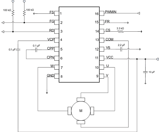 Figure 13. Typical Application Schematic
9.2.1 Design Requirements
Table 1. Design Parameters
| MIN | TYP | MAX | UNIT | ||
|---|---|---|---|---|---|
| Motor voltage | 5 | 16 | V | ||
| VCC capacitor | Place as close to the pin as possible | 10 | µF | ||
| Operating current | Running with normal load at rated speed | 1.5 | A | ||
| Absolute max current | During startup and locked motor condition | 2 | A | ||
9.2.2 Detailed Design Procedure
- Refer to the Design Requirements and ensure the system meets the recommended application range.
- Ensure the VCC level is in between 5 and 16 V
- Verify the motor needs no more than 1.5 A during runtime
- Follow the application and Power Supply Recommendations when constructing the schematic.
- If the motor is high current/ high speed, use three Schottky diodes between the phases and ground.
- Make sure there is adequate capacitance on VCC, V5, VCP, CPP, and CPN.
- Size the resistor on CS according to the details given in feature description.
- Use a pull-up on FG and RD.
- If the motor doesn’t have a common pin, create one using the method listed in Application Information.
- Build the hardware according to the Layout Guidelines.
- Place the supply capacitors as close to the pins as possible.
- Route the U, V, W, and VCC traces to handle the allowed current.
- Ensure GND connections are made with the pin and thermal PAD.
- Use vias on the thermal pad to dissipate heat away from the IC.
- Test the system with the application's motor to verify proper operation.
9.2.3 Application Curves
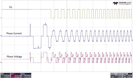 Figure 14. Startup Waveforms
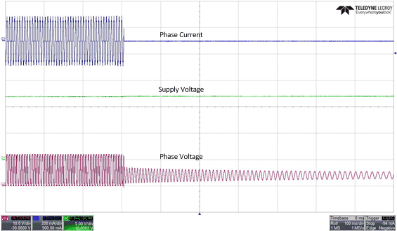 Figure 16. AVS Protection
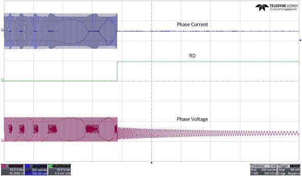 Figure 15. Lock Detection