SLWS237A November 2012 – November 2014 DRV11873
PRODUCTION DATA.
- 1 Features
- 2 Applications
- 3 Description
- 4 Simplified Schematic
- 5 Revision History
- 6 Pin Configuration and Functions
- 7 Specifications
- 8 Detailed Description
- 9 Application and Implementation
- 10Power Supply Recommendations
- 11Layout
- 12Device and Documentation Support
- 13Mechanical, Packaging, and Orderable Information
Package Options
Mechanical Data (Package|Pins)
- PWP|16
Thermal pad, mechanical data (Package|Pins)
- PWP|16
Orderable Information
7 Specifications
7.1 Absolute Maximum Ratings
over operating free-air temperature (unless otherwise noted)| MIN | MAX | UNIT | ||
|---|---|---|---|---|
| Input voltage(1) | VCC | –0.3 | 20 | V |
| CS | –0.3 | 3.6 | ||
| PWMIN, FS, FR | –0.3 | 6 | ||
| GND | –0.3 | 0.3 | ||
| COM | –1 | 20 | ||
| Output voltage(1) | U, V, W | –1 | 20 | V |
| FG, RD | –0.3 | 20 | ||
| VCP | –0.3 | 25 | ||
| CPN | –0.3 | 20 | ||
| CPP | –0.3 | 25 | ||
| V5 | –0.3 | 6 | ||
| TJ | Operating junction temperature | –40 | 125 | °C |
(1) Voltage values are with respect to the network ground terminal unless otherwise noted.
7.2 Handling Ratings
| MIN | MAX | UNIT | |||
|---|---|---|---|---|---|
| Tstg | Storage temperature range | –55 | 150 | °C | |
| V(ESD) | Electrostatic discharge | Human body model (HBM), per ANSI/ESDA/JEDEC JS-001, all pins(1) | –4000 | 4000 | V |
| Charged device model (CDM), per JEDEC specification JESD22-C101, all pins(2) | –1000 | 1000 | |||
| Machine model (MM) | –200 | 200 | |||
(1) JEDEC document JEP155 states that 500-V HBM allows safe manufacturing with a standard ESD control process.
(2) JEDEC document JEP157 states that 250-V CDM allows safe manufacturing with a standard ESD control process.
7.3 Recommended Operating Conditions
over operating free-air temperature range (unless otherwise noted)| MIN | MAX | UNIT | ||
|---|---|---|---|---|
| Supply voltage | VCC | 5 | 16 | V |
| Voltage range | U, V, W | –0.7 | 17 | V |
| COM | –0.1 | 17 | ||
| FG, RD | –0.1 | 16 | ||
| PGND, GND | –0.1 | 0.1 | ||
| VCP | –0.1 | 22 | ||
| CPP | –0.1 | 22 | ||
| CPN | –0.1 | 16 | ||
| V5 | –0.1 | 5.5 | ||
| PWMIN, FR, FS | –0.1 | 5.5 | ||
| TJ | Operating junction temperature | –40 | 125 | V |
7.4 Thermal Information
| THERMAL METRIC(1) | DRV11873 | UNIT | |
|---|---|---|---|
| PWP | |||
| 16 PINS | |||
| RθJA | Junction-to-ambient thermal resistance | 39.4 | °C/W |
| RθJC(top) | Junction-to-case (top) thermal resistance | 30.3 | |
| RθJB | Junction-to-board thermal resistance | 25.6 | |
| ψJT | Junction-to-top characterization parameter | 0.5 | |
| ψJB | Junction-to-board characterization parameter | 10.2 | |
| RθJC(bot) | Junction-to-case (bottom) thermal resistance | 3.6 | |
(1) For more information about traditional and new thermal metrics, see the IC Package Thermal Metrics application report, SPRA953.
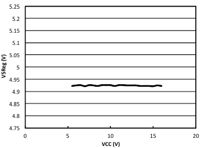
7.5 Electrical Characteristics
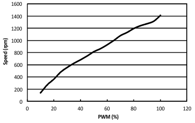
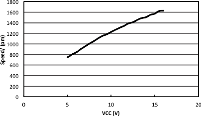
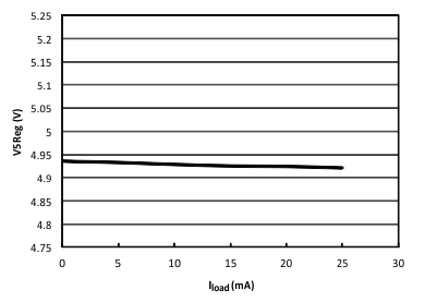
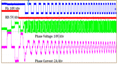
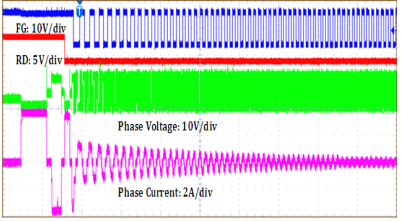
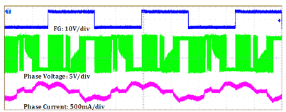
over recommended operating free-air temperature (unless otherwise noted)7.6 Typical Characteristics
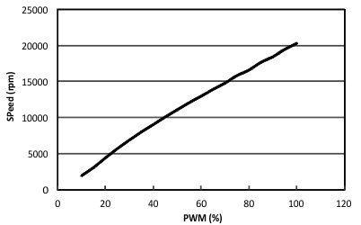
| Input voltage = 12 V | PWM duty = 100% | FS = 1 |
| t = 20 ms/div | ||
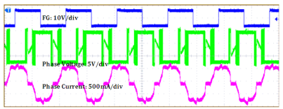
| Input voltage = 12 V | PWM duty = 100% | FS = 1 |
| t = 800 µs/div | ||
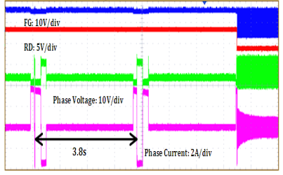
| Input voltage = 12 V | PWM duty = 100% | FS = 1 |
| t = 1 s/div |
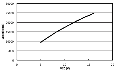
| Input voltage = 12 V | PWM duty = 10% | FS = 1 |
| t = 40 ms/div | ||
| Input voltage = 12 V | PWM duty = 50% | FS = 1 |
| t = 800 µs/div | ||
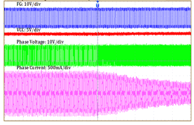
| Input voltage = 12 V | PWM duty switch from 100% to 20% | |
| t = 20 ms/div | FS = 1 | |