SLWS237A November 2012 – November 2014 DRV11873
PRODUCTION DATA.
- 1 Features
- 2 Applications
- 3 Description
- 4 Simplified Schematic
- 5 Revision History
- 6 Pin Configuration and Functions
- 7 Specifications
- 8 Detailed Description
- 9 Application and Implementation
- 10Power Supply Recommendations
- 11Layout
- 12Device and Documentation Support
- 13Mechanical, Packaging, and Orderable Information
Package Options
Mechanical Data (Package|Pins)
- PWP|16
Thermal pad, mechanical data (Package|Pins)
- PWP|16
Orderable Information
6 Pin Configuration and Functions
PWP Package
16 Pins
(Top View)
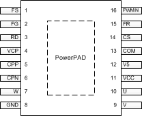
Pin Functions
| PIN | I/O(1) | DESCRIPTION | |
|---|---|---|---|
| NAME | NO. | ||
| FS | 1 | I | Motor parameter adjustment pin. Pull low for lower-speed motor and pull high for high-speed motor. |
| FG | 2 | O | Frequency generator output. The output period is equal to 6 electrical states (FG). |
| RD | 3 | O | In the lock condition, RD output is high through a pullup resistor to VCC or 5 V. |
| VCP | 4 | O | Charge pump output |
| CPP | 5 | O | Charge pump conversion terminal |
| CPN | 6 | O | Charge pump conversion terminal |
| W | 7 | O | Phase W output |
| GND | 8 | — | Ground pin |
| V | 9 | O | Phase V output |
| U | 10 | O | Phase U output |
| VCC | 11 | I | Input voltage for motor and chip supply voltage |
| V5 | 12 | O | 5-V regulator output |
| COM | 13 | I | Motor common terminal input. If the motor does not have a common wire, see Application and Implementation for more details. |
| CS | 14 | I | Overcurrent threshold set-up pin. A resistor set-up current limit is connected between this pin and ground. The voltage across the resistor compares with the voltage converted from the bottom MOSFETs' current. If MOSFETs' current is high, the part goes into the overcurrent protection mode by turning off the top PWM MOSFET and keeping the bottom MOSFET on. Ilimit(A) = 6600 / RCS (Ω); Equation valid range: 500 mA < Ilimit < 2000 mA |
| FR | 15 | I | Set high for reverse rotation. Set low or floating for forward rotation. |
| PWMIN | 16 | I | PWM input pin. The PWM input signal is converted to a fixed switching frequency on the MOSFET driver. |
(1) I = input, O = output, N/A = not available