SLVSB25C August 2011 – June 2015 DRV201
PRODUCTION DATA.
- 1 Features
- 2 Applications
- 3 Description
- 4 Revision History
- 5 Pin Configuration and Functions
- 6 Specifications
-
7 Detailed Description
- 7.1 Overview
- 7.2 Functional Block Diagram
- 7.3 Feature Description
- 7.4 Device Functional Modes
- 7.5 Programming
- 7.6
Register Maps
- 7.6.1 Register Address Map
- 7.6.2 Control Register (Control) Address - 0x02h
- 7.6.3 VCM MSB Current Control Register (VCM_Current_MSB) Address - 0x03h
- 7.6.4 VCM LSB Current Control Register (VCM_Current_LSB) Address - 0x04h
- 7.6.5 Status Register (Status) Address - 0x05h
- 7.6.6 Mode Register (Mode) Address - 0x06h
- 7.6.7 VCM Resonance Frequency Register (VCM_FREQ) Address - 0x07h
- 8 Application and Implementation
- 9 Power Supply Recommendations
- 10Layout
- 11Device and Documentation Support
- 12Mechanical, Packaging, and Orderable Information
Package Options
Mechanical Data (Package|Pins)
Thermal pad, mechanical data (Package|Pins)
Orderable Information
8 Application and Implementation
NOTE
Information in the following applications sections is not part of the TI component specification, and TI does not warrant its accuracy or completeness. TI’s customers are responsible for determining suitability of components for their purposes. Customers should validate and test their design implementation to confirm system functionality.
8.1 Application Information
The DRV201 device is a voice coil motor driver designed for camera auto focus control. The device allows for a highly efficient PWM current control for VCM, while reducing lens ringing in order to significantly lower the time needed for the lens to auto focus. The following design is a common application of the DRV201 device.
8.1.1 VCM Mechanical Ringing Frequency
Ringing compensation is dependent on the VCM resonance frequency, and this can be controlled through the VCM_FREQ register (07h) from 50 Hz up to 150 Hz. VCM mechanical ringing frequency for the ringing compensation can be selected using Equation 3. The formula gives the VCM_FREQ[7:0] register value in decimal which should be rounded to the nearest integer.

Default VCM mechanical ringing frequency is 76.4 Hz.

8.2 Typical Application
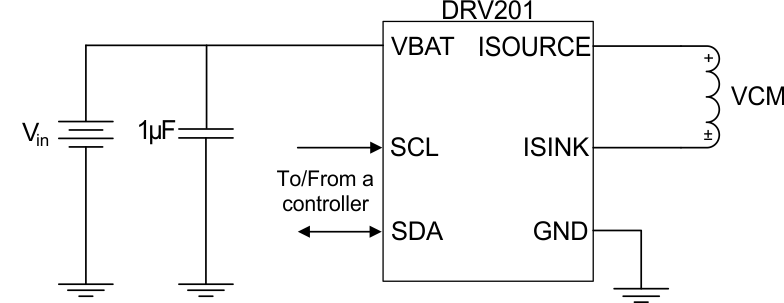 Figure 20. Typical Application Schematic
8.2.1 Design Requirements
Table 8. Design Parameters
| DESIGN PARAMETER | REFERENCE | EXAMPLE VALUE |
|---|---|---|
| Supply voltage | Vin | 3.7 |
| Motor Winding Resistance | RL | 15 Ω |
| Motor Winding Inductance | IL | 100 µH |
| Actuator Size | 8.5 x 8.5 x 3.4 (mm) | |
| Lens in the VCM | M6 (Pitch: 0.35) | |
| Weight of VCM | 75 mg | |
| TTL | 4.2 mm | |
| FB | 1.1 mm |
8.2.2 Detailed Design Procedure
8.2.2.1 User Example 1
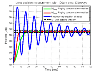
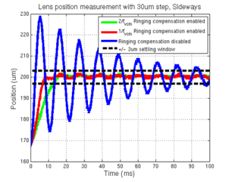
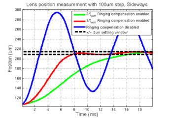
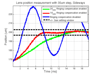
In Figure 21, lens settling time and settling window shows how lens control is defined. Below is an example case how the lens is controlled and what settling time is achieved:
Measured VCM resonance frequency = 100 Hz
- According to Table 1, VCM_FREQ[7:0] = ‘10111111’ (reg 0x07h)
VCM resonance frequency, fVCM, variation is within ±10% (minimum 90 Hz, maximum 110 Hz)
- 1/fVCM ringing compensation is used : RING_MODE = ‘1’ (reg 0x06h)
Stepping the lens by 50 µm
- The lens is settled into a ±5-µm window within 10 ms (1/fVCM)
8.2.2.2 User Example 2
If the case is otherwise exactly the same, but VCM resonance frequency cannot be guaranteed to stay at more than ±30% variation, slower ringing compensation should be used:
Measured VCM resonance frequency = 100 Hz
- According to Table 1, VCM_FREQ[7:0] = ‘10111111’ (reg 0x07h)
VCM resonance frequency, fVCM, variation is within ±30% (minimum 70 Hz, maximum 130 Hz)
- 2/fVCM ringing compensation is used : RING_MODE = ‘0’ (reg 0x06h)
Stepping the lens by 50 µm
- The lens is settled into a ±5-µm window within 20 ms (2/fVCM)
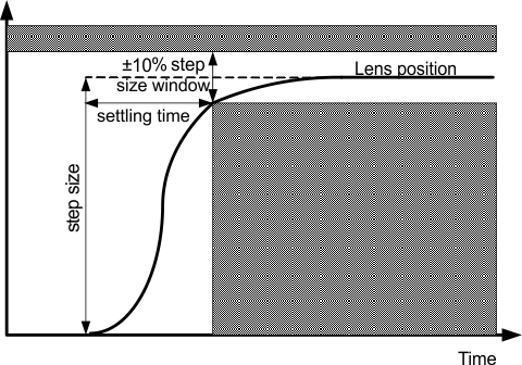 Figure 21. Lens Settling Time and Settling Window
8.2.3 Application Curves
