SLVSBA5D October 2012 – April 2016 DRV8313
PRODUCTION DATA.
- 1 Features
- 2 Applications
- 3 Description
- 4 Revision History
- 5 Pin Configuration and Functions
- 6 Specifications
- 7 Detailed Description
- 8 Application and Implementation
- 9 Power Supply Recommendations
- 10Layout
- 11Device and Documentation Support
- 12Mechanical, Packaging, and Orderable Information
Package Options
Mechanical Data (Package|Pins)
Thermal pad, mechanical data (Package|Pins)
Orderable Information
8 Application and Implementation
NOTE
Information in the following applications sections is not part of the TI component specification, and TI does not warrant its accuracy or completeness. TI’s customers are responsible for determining suitability of components for their purposes. Customers should validate and test their design implementation to confirm system functionality.
8.1 Application Information
The DRV8313 can be used to drive Brushless-DC motors, Brushed-DC motors, and solenoid loads. The following design procedure can be used to configure the DRV8313.
8.2 Typical Applications
8.2.1 Three-Phase Brushless-DC Motor Control
In this application, the DRV8313 is used to drive a Brushless-DC motor
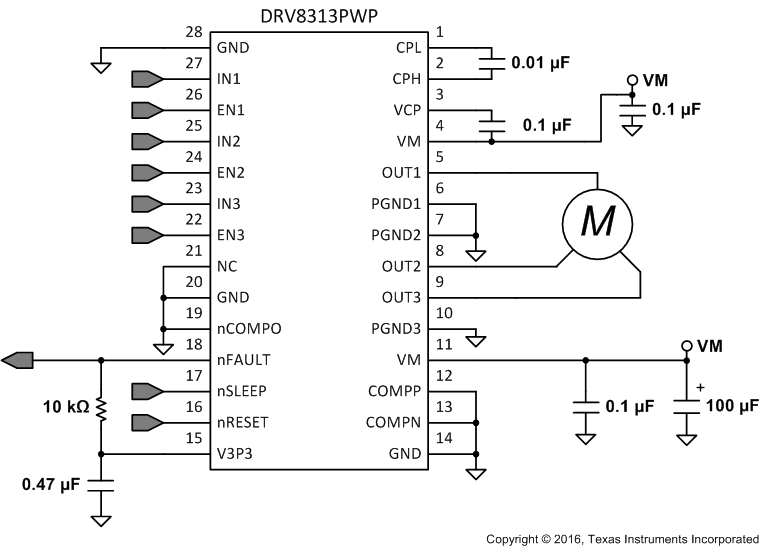 Figure 13. BLDC Driver Application Schematic
8.2.1.1 Design Requirements
Table 4 gives design input parameters for system design.
Table 4. Design Parameters
| DESIGN PARAMETER | REFERENCE | EXAMPLE VALUE |
|---|---|---|
| Typical supply voltage | VM | 18 V |
| Maximum voltage | VMMAX | 36 V |
| Target rms current | IRMS | 1.2 A |
| Motor winding resistance | MR | 0.5 Ω |
| Motor winding inductance | ML | 0.28 mH |
| Motor poles | MP | 16 poles |
| Motor rated RPM | MRPM | 4000 RPM |
| PWM frequency | fPWM | 25 kHz |
8.2.1.2 Detailed Design Procedure
8.2.1.2.1 Motor Voltage
Brushless-DC motors are typically rated for a certain voltage (for example 12 V and 24 V). Operating a motor at a higher voltage corresponds to a lower drive current to obtain the same motor power. A higher operating voltage also corresponds to a higher obtainable rpm. DRV8313 allows for the use of higher operaing voltage because of a maximum VM rating of 60 V.
Operating at lower voltages generally allows for more accurate control of phase currents. The DRV8313 functions down to a supply of 8 V.
8.2.1.2.2 Motor Commutation
The DRV8313 can drive both trapezoidal (120°) and sinusiodal (180°) commutation due to independent control of each of the three 1/2-H bridges.
Both synchronous and asynchronous rectification are supported. Synchronous rectification is achieved by applying a pulse-width-modulated (PWM) input signal to the INx pins while driving. The user can also implement asynchronous rectification by applying the PWM signal to the ENx inputs.
Table 5. Trapezoidal (120°) Commutation States
| State | OUT1 (Phase U) | OUT2 (Phase V) | OUT3 (Phase W) | ||||||
|---|---|---|---|---|---|---|---|---|---|
| IN1 | EN1 | OUT1 | IN2 | EN2 | OUT2 | IN3 | EN3 | OUT3 | |
| 1 | X | 0 | Z | 1 | 1 | H | 0 | 1 | L |
| 2 | 1 | 1 | H | X | 0 | Z | 0 | 1 | L |
| 3 | 1 | 1 | H | 0 | 1 | L | X | 0 | Z |
| 4 | X | 0 | Z | 0 | 1 | L | 1 | 1 | H |
| 5 | 0 | 1 | L | X | 0 | Z | 1 | 1 | H |
| 6 | 0 | 1 | L | 1 | 1 | H | X | 0 | Z |
| Brake | 0 | 1 | L | 0 | 1 | L | 0 | 1 | L |
| Coast | X | 0 | Z | X | 0 | Z | X | 0 | Z |
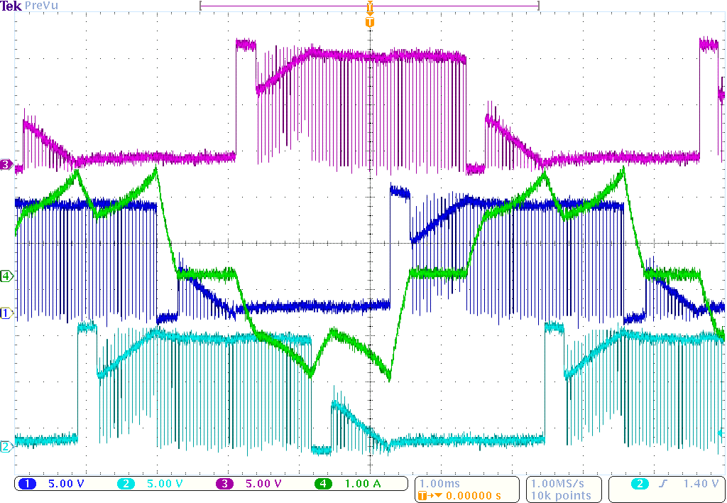
8.2.1.3 Application Curve
8.2.2 Three-Phase Brushless-DC Motor Control With Current Monitor
In this application, the DRV8313 is used to drive a brushless-DC motor and the uncommitted comparator is used to monitor the motor current
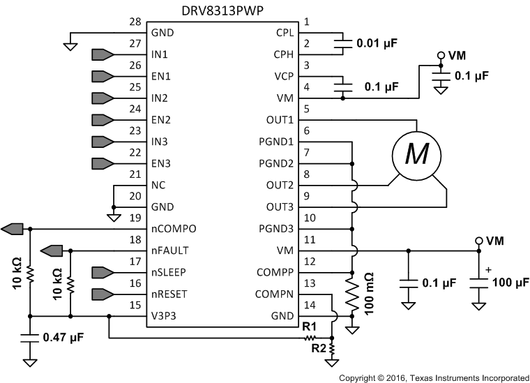 Figure 15. Uncommitted Comparator Used As a Current Monitor
8.2.2.1 Design Requirements
Table 6 gives design input parameters for system design.
Table 6. Design Parameters
| DESIGN PARAMETER | REFERENCE | EXAMPLE VALUE |
|---|---|---|
| Trip current | ITRIP | 2.5 A |
8.2.2.2 Detailed Design Procedure
8.2.2.2.1 Trip Current
The uncommitted comparator is configured such that the negative input COMPN is connected to the PGNDx pins. A sense resistor is placed from the PGNDx/COMPN pins to GND.
The voltage on the COMPP pin will set the current monitor trip threshold. In this case, the the nCOMPO pin will change state when COMPP and COMPN have the same potential.

| Example: If the desired trip current is 2.5 A | ||
| Set RSENSE = 200 mΩ | ||
| COMPN would have to be 0.5 V. | ||
| Create a resistor divider from V3P3 (3.3 V) to set COMPN ≈ 0.5 V. | ||
| Set R2 = 10 kΩ, set R1 = 56 kΩ | ||
8.2.2.2.2 Sense Resistor
For optimal performance, the sense resistor must have the following characteristics:
- Surface-mount
- Low inductance
- Rated for high enough power
- Placed closely to the motor driver
The power dissipated by the sense resistor equals Irms 2 × R. For example, if the rms motor current is 1 A and a 200-mΩ sense resistor is used, the resistor will dissipate 1 A2 × 0.2 Ω = 0.2 W. The power quickly increases with higher current levels.
Resistors typically have a rated power within some ambient temperature range, along with a derated power curve for high ambient temperatures. When a PCB is shared with other components generating heat, margin should be added. Measuring the actual sense-resistor temperature in a final system, along with the power MOSFETs, is always best because these are often the hottest components.
Because power resistors are larger and more expensive than standard resistors, using multiple standard resistors in parallel, between the sense node and ground is a common practice. This configuration distributes the current and heat dissipation.
8.2.3 Brushed-DC and Solenoid Load
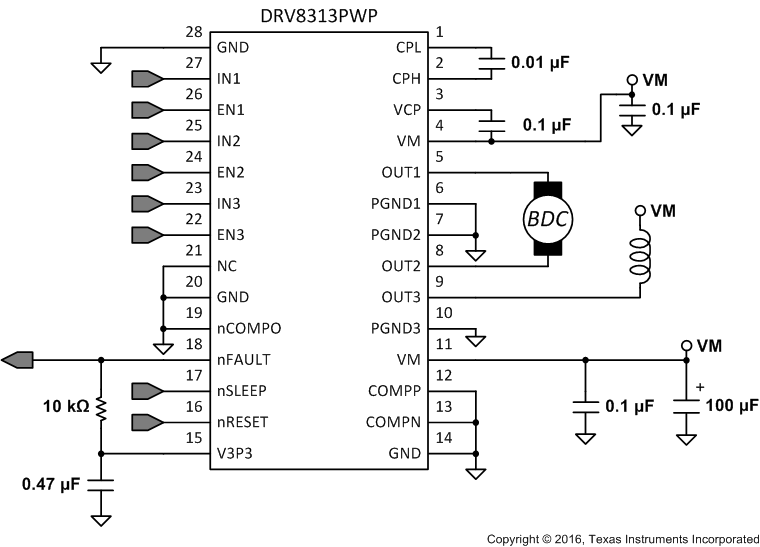 Figure 16. Brushed-DC and Solenoid Schematic
8.2.3.1 Design Requirements
Table 7 gives design input parameters for system design.
Table 7. Design Parameters
| DESIGN PARAMETER | REFERENCE | EXAMPLE VALUE |
|---|---|---|
| Brushed motor rms current | IRMS, BDC | 1.0 A |
| Brushed motor peak current | IPEAK, BDC | 2.0 A |
| Solenoid rms current | IRMS, SOL | 0.5 A |
| Solenoid peak current | IPEAK, SOL | 1.0 A |
8.2.3.1.1 Detailed Design Procedure
Table 8. Brushed-DC Control
| Function | IN1 | EN1 | IN2 | EN2 | OUT1 | OUT2 |
|---|---|---|---|---|---|---|
| Forward | 1 | 1 | 0 | 1 | H | L |
| Reverse | 0 | 1 | 1 | 1 | L | H |
| Brake (low-side slow decay) | 0 | 1 | 0 | 1 | L | L |
| High-side slow decay | 1 | 1 | 1 | 1 | H | H |
| Coast | X | 0 | X | 0 | Z | Z |
Table 9. Solenoid Control (High-Side Load)
| Function | IN3 | EN3 | OUT3 |
|---|---|---|---|
| Coast / Off | X | 0 | Z |
| On | 0 | 1 | L |
| Brake | 1 | 1 | H |
8.2.4 Three Solenoid Loads
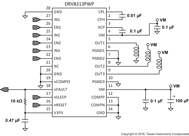 Figure 17. Three Independent Load Connections Schematic
8.2.4.1 Design Requirements
Table 10 gives design input parameters for system design.
Table 10. Design Parameters
| DESIGN PARAMETER | REFERENCE | EXAMPLE VALUE |
|---|---|---|
| Solenoid rms current | IRMS, SOL | 1.0 A |
| Solenoid peak current | IPEAK, SOL | 1.5 A |
8.2.4.1.1 Detailed Design Procedure
Table 11. Solenoid Control (high-side load)
| Function | IN2 | EN2 | OUT2 |
|---|---|---|---|
| Coast / Off | X | 0 | Z |
| On | 0 | 1 | L |
| Brake | 1 | 1 | H |
Table 12. Solenoid Control (low-side load)
| Function | IN1 | EN1 | OUT1 |
|---|---|---|---|
| Coast / Off | X | 0 | Z |
| On | 1 | 1 | H |
| Brake | 0 | 1 | L |