SLVSBA5D October 2012 – April 2016 DRV8313
PRODUCTION DATA.
- 1 Features
- 2 Applications
- 3 Description
- 4 Revision History
- 5 Pin Configuration and Functions
- 6 Specifications
- 7 Detailed Description
- 8 Application and Implementation
- 9 Power Supply Recommendations
- 10Layout
- 11Device and Documentation Support
- 12Mechanical, Packaging, and Orderable Information
Package Options
Mechanical Data (Package|Pins)
Thermal pad, mechanical data (Package|Pins)
Orderable Information
7 Detailed Description
7.1 Overview
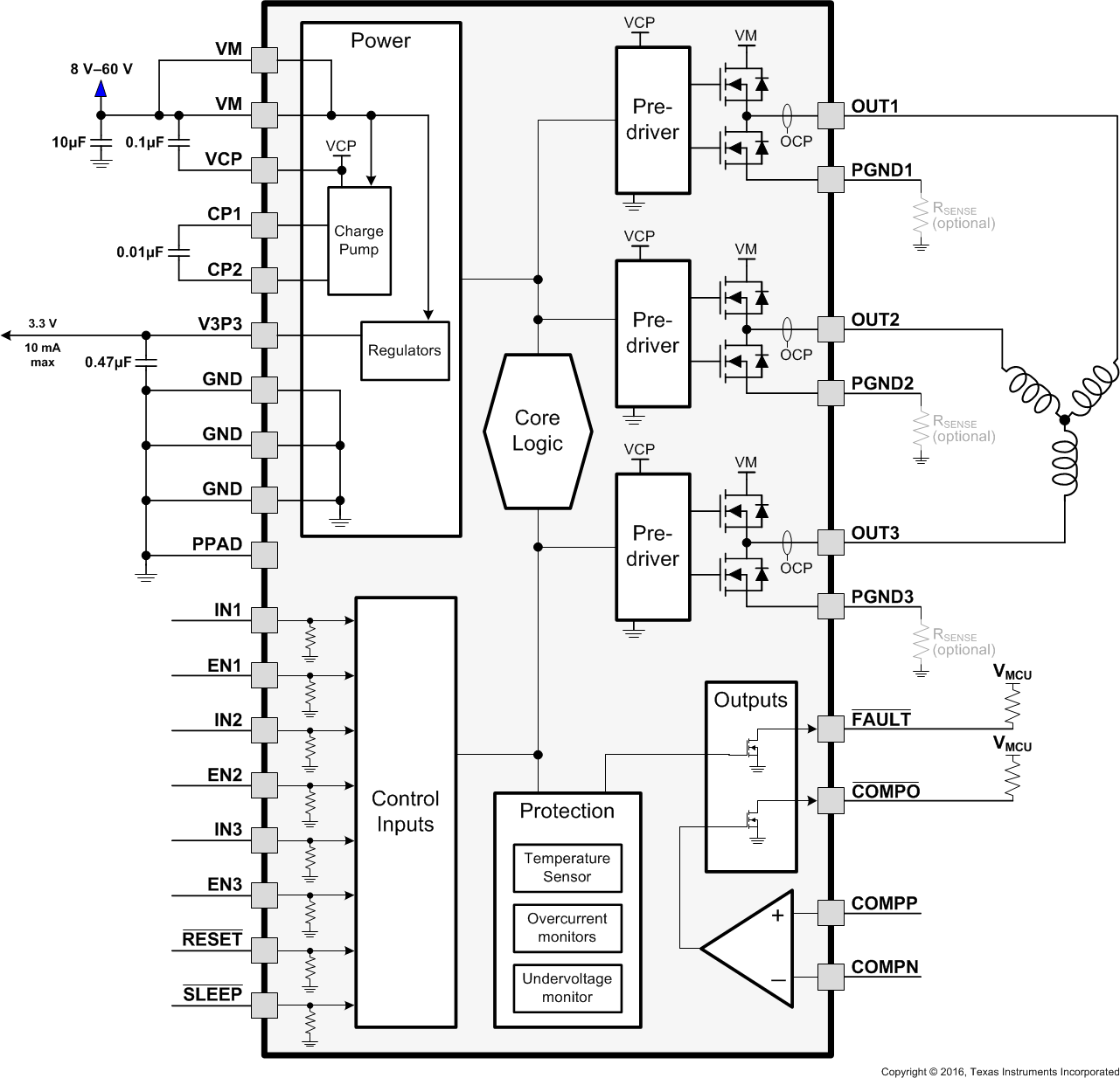
The DRV8313 integrates three independent 2.5-A half-H bridges, protection circuits, sleep mode, fault reporting, and a comparator. The single power supply supports a wide 8-V to 60-V range, making it well-suited for motor drive applications.
7.2 Functional Block Diagram

7.3 Feature Description
7.3.1 Output Stage
The DRV8313 contains three half-H-bridge drivers. The source terminals of the low-side FETs of all three half-H-bridges terminate at separate pins (PGND1, PGND2, and PGND3) to allow the use of a low-side current-sense resistor on each output, if desired. The user can also connect all three together to a single low-side sense resistor, or can connect them directly to ground if current sensing is unneeded.
If using a low-side sense resistor, ensure that the voltage on the PGND1, PGND2, or PGND3 pin does not exceed ±500 mV.
The device has two VM motor power-supply pins. Connect both VM pins together to the motor-supply voltage.
7.3.2 Bridge Control
The INx input pins directly control the state (high or low) of the OUTx outputs; the ENx input pins enable or disable the OUTx driver. Table 1 shows the logic:
Table 1. Logic States
| INx | ENx | OUTx |
|---|---|---|
| X | 0 | Z |
| 0 | 1 | L |
| 1 | 1 | H |
7.3.3 Charge Pump
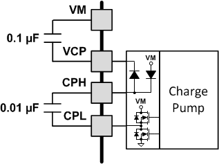
Because the output stages use N-channel FETs, the device requires a gate-drive voltage higher than the VM power supply to enhance the high-side FETs fully. The DRV8313 integrates a charge-pump circuit that generates a voltage above the VM supply for this purpose.
The charge pump requires two external capacitors for operation. See the block diagram and pin descriptions for details on these capacitors (value, connection, and so forth).
The charge pump shuts down when nSLEEP is low.
 Figure 11. DRV8313 Charge Pump
7.3.4 Comparator
The DRV8313 includes an uncommitted comparator, which can find use as a current-limit comparator or for other purposes.
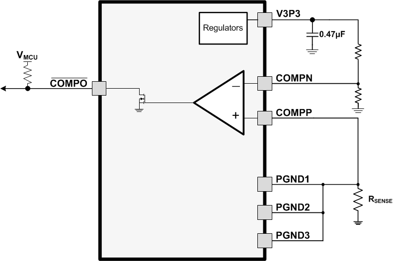
Figure 12 shows connections to use the comparator to sense current for implementing a current limit. Current from all three low-side FETs is sensed using a single low-side sense resistor. The voltage across the sense resistor is compared with a reference, and when the sensed voltage exceeds the reference, a current-limit condition is signaled to the controller. The V3P3 internal voltage regulator can be used to set the reference voltage of the comparator.
 Figure 12. Comparator As Current Monitor
7.3.5 Protection Circuits
The DRV8313 has full protection against undervoltage, overcurrent, and overtemperature events.
7.3.5.1 Undervoltage Lockout (UVLO)
If at any time the voltage on the VM pin falls below the undervoltage threshold voltage (VUVLO), all FETs in the H-bridge will be disabled, the charge pump will be disabled, the internal logic is reset, and the nFAULT pin will be driven low. Operation will resume when VM rises above the UVLO threshold. The nFAULT pin will be released after operation has resumed.
7.3.5.2 Thermal Shutdown (TSD)
If the die temperature exceeds safe limits, all FETs in the H-bridge will be disabled and the nFAULT pin will be driven low. Once the die temperature has fallen to a safe level operation will automatically resume. The nFAULT pin will be released after operation has resumed.
7.3.5.3 Overcurrent Protection (OCP)
An analog current limit circuit on each FET limits the current through the FET by removing the gate drive. If this analog current limit persists for longer than tOCP, the device disables the channel experiencing the overcurrent and drives the nFAULT pin low. The driver remains off until either assertion of nRESET or the cycling of VM power.
Overcurrent conditions on both high- and low-side devices, that is, a short to ground, supply, or across the motor winding, all result in an overcurrent shutdown.
Table 2. Fault Condition Summary
| FAULT | CONDITION | ERROR REPORT | H-BRIDGE | CHARGE PUMP | V3P3 | RECOVERY |
|---|---|---|---|---|---|---|
| VM undervoltage (UVLO) |
VM < VUVLO
(max 8 V) |
nFAULT | Disabled | Disabled |
Operating |
VM > VUVLO
(max 8 V) |
| Thermal Shutdown (TSD) |
TJ > TTSD
(min 150°C) |
nFAULT | Disabled | Operating |
Operating |
TJ < TTSD - THYS
(THYS typ 35°C) |
| Overcurrent (OCP) |
IOUT > IOCP
(min 3 A) |
nFAULT | Disabled | Operating |
Operating |
nRESET |
7.4 Device Functional Modes
The DRV8313 is active unless the nSLEEP pin is brought logic low. In sleep mode the charge pump is disabled, the output FETs are disabled Hi-Z, and the V3P3 regulator is disabled. The DRV313 is brought out of sleep mode automatically if nSLEEP is brought logic high.
7.4.1 nRESET and nSLEEP Operation
The nRESET pin, when driven low, resets any faults. It also disables the output drivers while it is active. The device ignores all inputs while nRESET is active. Note that there is an internal power-up-reset circuit, so that driving nRESET at power up is not required.
Driving nSLEEP low puts the device into a low-power sleep state. Entering this state disables the output drivers, stops the gate-drive charge pump, resets all internal logic (including faults), and stops all internal clocks. In this state, the device ignores all inputs until nSLEEP returns inactive-high. When returning from sleep mode, some time (approximately 1 ms) must pass before the motor driver becomes fully operational. The V3P3 regulator remains operational in sleep mode.
Table 3. Functional Modes Summary
| FAULT | CONDITION | H-BRIDGE | CHARGE PUMP | V3P3 |
|---|---|---|---|---|
| Operating | 8 V < VM < 60 V nSLEEP pin = 1 |
Operating | Operating | Operating |
| Sleep mode | 8 V < VM < 60 V nSLEEP pin = 0 |
Disabled | Disabled | Disabled |
| Fault encountered | VM undervoltage (UVLO) | Disabled | Disabled | Operating |
| Overcurrent (OCP) | Disabled | Operating | Operating | |
| Thermal shutdown (TSD) | Disabled | Operating | Operating |