SLVSH52 February   2023 DRV8316C-Q1

PRODUCTION DATA  

  1. Features
  2. Applications
  3. Description
  4. Revision History
  5. Device Comparison Table
  6. Pin Configuration and Functions
  7. Specifications
    1. 7.1 Absolute Maximum Ratings
    2. 7.2 ESD Ratings Auto
    3. 7.3 Recommended Operating Conditions
    4. 7.4 Thermal Information
    5. 7.5 Electrical Characteristics
    6. 7.6 SPI Timing Requirements
    7. 7.7 SPI Slave Mode Timings
    8. 7.8 Typical Characteristics
  8. Detailed Description
    1. 8.1 Overview
    2. 8.2 Functional Block Diagram
    3. 8.3 Feature Description
      1. 8.3.1  Output Stage
      2. 8.3.2  Control Modes
        1. 8.3.2.1 6x PWM Mode (PWM_MODE = 00b or MODE Pin Tied to AGND)
        2. 8.3.2.2 3x PWM Mode (PWM_MODE = 10b or MODE Pin is Connected to AVDD with RMODE)
        3. 8.3.2.3 Current Limit Mode (PWM_MODE = 01b / 11b or MODE Pin is Hi-Z or Connected to AVDD)
      3. 8.3.3  Device Interface Modes
        1. 8.3.3.1 Serial Peripheral Interface (SPI)
        2. 8.3.3.2 Hardware Interface
      4. 8.3.4  Step-Down Mixed-Mode Buck Regulator
        1. 8.3.4.1 Buck in Inductor Mode
        2. 8.3.4.2 Buck in Resistor mode
        3. 8.3.4.3 Buck Regulator with External LDO
        4. 8.3.4.4 AVDD Power Sequencing on Buck Regulator
        5. 8.3.4.5 Mixed mode Buck Operation and Control
      5. 8.3.5  AVDD Linear Voltage Regulator
      6. 8.3.6  Charge Pump
      7. 8.3.7  Slew Rate Control
      8. 8.3.8  Cross Conduction (Dead Time)
      9. 8.3.9  Propagation Delay
        1. 8.3.9.1 Driver Delay Compensation
      10. 8.3.10 Pin Diagrams
        1. 8.3.10.1 Logic Level Input Pin (Internal Pulldown)
        2. 8.3.10.2 Logic Level Input Pin (Internal Pullup)
        3. 8.3.10.3 Open Drain Pin
        4. 8.3.10.4 Push Pull Pin
        5. 8.3.10.5 Four Level Input Pin
      11. 8.3.11 Current Sense Amplifiers
        1. 8.3.11.1 Current Sense Amplifier Operation
      12. 8.3.12 Active Demagnetization
        1. 8.3.12.1 Automatic Synchronous Rectification Mode (ASR Mode)
          1. 8.3.12.1.1 Automatic Synchronous Rectification in Commutation
          2. 8.3.12.1.2 Automatic Synchronous Rectification in PWM Mode
        2. 8.3.12.2 Automatic Asynchronous Rectification Mode (AAR Mode)
      13. 8.3.13 Cycle-by-Cycle Current Limit
        1. 8.3.13.1 Cycle by Cycle Current Limit with 100% Duty Cycle Input
      14. 8.3.14 Protections
        1. 8.3.14.1 VM Supply Undervoltage Lockout (NPOR)
        2. 8.3.14.2 AVDD Undervoltage Lockout (AVDD_UV)
        3. 8.3.14.3 Buck Undervoltage Lockout (BUCK_UV)
        4. 8.3.14.4 VCP Charge Pump Undervoltage Lockout (CPUV)
        5. 8.3.14.5 Overvoltage Protection (OVP)
        6. 8.3.14.6 Overcurrent Protection (OCP)
          1. 8.3.14.6.1 OCP Latched Shutdown (OCP_MODE = 00b)
          2. 8.3.14.6.2 OCP Automatic Retry (OCP_MODE = 01b)
          3. 8.3.14.6.3 OCP Report Only (OCP_MODE = 10b)
          4. 8.3.14.6.4 OCP Disabled (OCP_MODE = 11b)
        7. 8.3.14.7 Buck Overcurrent Protection
        8. 8.3.14.8 Thermal Warning (OTW)
        9. 8.3.14.9 Thermal Shutdown (OTSD)
          1. 8.3.14.9.1 OTSD FET
          2. 8.3.14.9.2 OTSD (Non-FET)
    4. 8.4 Device Functional Modes
      1. 8.4.1 Functional Modes
        1. 8.4.1.1 Sleep Mode
        2. 8.4.1.2 Operating Mode
        3. 8.4.1.3 Fault Reset (CLR_FLT or nSLEEP Reset Pulse)
      2. 8.4.2 DRVOFF functionality
    5. 8.5 SPI Communication
      1. 8.5.1 Programming
        1. 8.5.1.1 SPI Format
    6. 8.6 Register Map
      1. 8.6.1 STATUS Registers
      2. 8.6.2 CONTROL Registers
  9. Application and Implementation
    1. 9.1 Application Information
    2. 9.2 Typical Applications
      1. 9.2.1 Three-Phase Brushless-DC Motor Control
        1. 9.2.1.1 Detailed Design Procedure
          1. 9.2.1.1.1 Motor Voltage
          2. 9.2.1.1.2 Using Active Demagnetization
          3. 9.2.1.1.3 Driver Propagation Delay and Dead Time
          4. 9.2.1.1.4 Using Delay Compensation
          5. 9.2.1.1.5 Using the Buck Regulator
          6. 9.2.1.1.6 Current Sensing and Output Filtering
        2. 9.2.1.2 Application Curves
      2. 9.2.2 Three-Phase Brushless-DC Motor Control With Current Limit
        1. 9.2.2.1 Block Diagram
        2. 9.2.2.2 Detailed Design Procedure
          1. 9.2.2.2.1 Motor Voltage
          2. 9.2.2.2.2 ILIM Implementation
        3. 9.2.2.3 Application Curves
      3. 9.2.3 Brushed-DC and Solenoid Load
        1. 9.2.3.1 Block Diagram
        2. 9.2.3.2 Design Requirements
          1. 9.2.3.2.1 Detailed Design Procedure
      4. 9.2.4 Three Solenoid Loads
        1. 9.2.4.1 Block Diagram
        2. 9.2.4.2 Design Requirements
          1. 9.2.4.2.1 Detailed Design Procedure
  10. 10Power Supply Recommendations
    1. 10.1 Bulk Capacitance
  11. 11Layout
    1. 11.1 Layout Guidelines
    2. 11.2 Layout Example
    3. 11.3 Thermal Considerations
      1. 11.3.1 Power Dissipation
  12. 12Device and Documentation Support
    1. 12.1 Documentation Support
      1. 12.1.1 Related Documentation
    2. 12.2 Support Resources
    3. 12.3 Trademarks
    4. 12.4 Electrostatic Discharge Caution
    5. 12.5 Glossary
  13. 13Mechanical, Packaging, and Orderable Information

Package Options

Mechanical Data (Package|Pins)
Thermal pad, mechanical data (Package|Pins)
Orderable Information

Cycle-by-Cycle Current Limit

The current-limit circuit activates if the current flowing through the low-side MOSFET exceeds the ILIMIT current. This feature restricts motor current to less than the ILIMIT.

The current-limit circuitry utilizes the current sense amplifier output of the three phases compared with the voltage at ILIM pin. #FIG_MW5_GZJ_F4B shows the implementation of current limit circuitry. As shown in this figure, the output of current sense amplifiers is combined with star connected resistive network. This measured voltage VMEAS is compared with the external reference voltage e VILIM pin to realize the current limit implementation. The relation between current sensed on OUTX pin and VMEAS threshold is given as:

Equation 5. GUID-20210105-CA0I-NGVC-JP9V-H5JZKB0ZR76Z-low.gif

where

  • AVDD is 3.3-V LDO output
  • OUTX is current flowing into the low-side MOSFET
  • GAIN is the CSA_GAIN setting

The ILIMIT threshold can be adjusted by configuring ILIM pin between AVDD/2 to (AVDD/2 - 0.4) V. AVDD/2 is minimum value and when it is applied on ILIM pin cycle by cycle current limit is disabled, whereas maximum threshold of 8 A can be configured by applying (AVDD/2 - 0.4) V on ILIM pin.
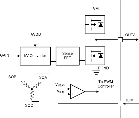
GUID-20210105-CA0I-TGTD-NXR6-L3ZCXQFS8N8L-low.gif Figure 8-36 Current Limit Implementation

When then the current limit activates, the high-side FET is disabled until the beginning of the next PWM cycle as shown in #X857-2. The low-side FETs can operate in brake mode or high-Z mode by configuring the ILIM_RECIR bit in the SPI device variant.
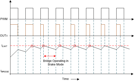
GUID-4E683246-4346-45BA-91D7-439DB22E3591-low.gif Figure 8-37 Cycle-by-Cycle Current-Limit Operation