SLVSGX4B June 2022 – December 2024 DRV8329
PRODUCTION DATA
- 1
- 1 Features
- 2 Applications
- 3 Description
- 4 Device Comparison Table
- 5 Pin Configuration and Functions
- 6 Specification
-
7 Detailed Description
- 7.1 Overview
- 7.2 Functional Block Diagram
- 7.3
Feature Description
- 7.3.1 Three BLDC Gate Drivers
- 7.3.2 AVDD Linear Voltage Regulator
- 7.3.3 Pin Diagrams
- 7.3.4 Low-Side Current Sense Amplifiers
- 7.3.5 Gate Driver Shutdown Sequence (DRVOFF)
- 7.3.6
Gate Driver Protective Circuits
- 7.3.6.1 PVDD Supply Undervoltage Lockout (PVDD_UV)
- 7.3.6.2 AVDD Power on Reset (AVDD_POR)
- 7.3.6.3 GVDD Undervoltage Lockout (GVDD_UV)
- 7.3.6.4 BST Undervoltage Lockout (BST_UV)
- 7.3.6.5 MOSFET VDS Overcurrent Protection (VDS_OCP)
- 7.3.6.6 VSENSE Overcurrent Protection (SEN_OCP)
- 7.3.6.7 Thermal Shutdown (OTSD)
- 7.4 Device Functional Modes
-
8 Application and Implementation
- 8.1 Application Information
- 8.2
Typical Application
- 8.2.1
Three Phase Brushless-DC Motor Control
- 8.2.1.1
Detailed Design Procedure
- 8.2.1.1.1 Motor Voltage
- 8.2.1.1.2 Bootstrap Capacitor and GVDD Capacitor Selection
- 8.2.1.1.3 Gate Drive Current
- 8.2.1.1.4 Gate Resistor Selection
- 8.2.1.1.5 System Considerations in High Power Designs
- 8.2.1.1.6 Dead Time Resistor Selection
- 8.2.1.1.7 VDSLVL Selection
- 8.2.1.1.8 AVDD Power Losses
- 8.2.1.1.9 Current Sensing and Output Filtering
- 8.2.1.1.10 Power Dissipation and Junction Temperature Losses
- 8.2.1.1
Detailed Design Procedure
- 8.2.2 Application Curves
- 8.2.1
Three Phase Brushless-DC Motor Control
- 8.3 Power Supply Recommendations
- 8.4 Layout
- 9 Device and Documentation Support
- 10Revision History
- 11Mechanical, Packaging, and Orderable Information
Package Options
Mechanical Data (Package|Pins)
- REE|36
Thermal pad, mechanical data (Package|Pins)
Orderable Information
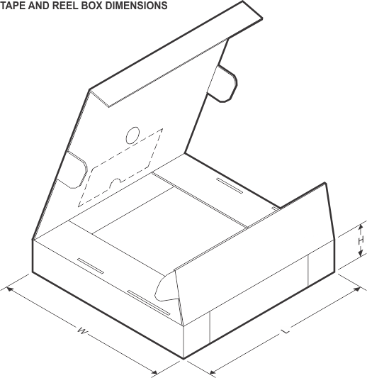
11.1 Tape and Reel Information

| Device | Package Type |
Package Drawing | Pins | SPQ | Reel Diameter (mm) |
Reel Width W1 (mm) |
A0 (mm) |
B0 (mm) |
K0 (mm) |
P1 (mm) |
W (mm) |
Pin1 Quadrant |
|---|---|---|---|---|---|---|---|---|---|---|---|---|
| PDRV8329AREER | WQFN | REE | 36 | 5000 | 330.0 | 12.4 | 4.3 | 5.3 | 1.3 | 8.0 | 12.0 | Q1 |
| Device | Package Type | Package Drawing | Pins | SPQ | Length (mm) | Width (mm) | Height (mm) |
|---|---|---|---|---|---|---|---|
| PDRV8329AREER | WQFN | REE | 36 | 5000 | 367.0 | 367.0 | 35.0 |