SLVSDR9E October 2016 – January 2021 DRV8702-Q1 , DRV8703-Q1
PRODUCTION DATA
- 1 Features
- 2 Applications
- 3 Description
- 4 Revision History
- 5 Pin Configuration and Functions
- 6 Specifications
-
7 Detailed Description
- 7.1 Overview
- 7.2 Functional Block Diagram
- 7.3
Feature Description
- 7.3.1 Bridge Control
- 7.3.2 MODE Pin
- 7.3.3 nFAULT Pin
- 7.3.4 Current Regulation
- 7.3.5 Amplifier Output (SO)
- 7.3.6 PWM Motor Gate Drivers
- 7.3.7 IDRIVE Pin (DRV8702-Q1 Only)
- 7.3.8 Dead Time
- 7.3.9 Propagation Delay
- 7.3.10 Overcurrent VDS Monitor
- 7.3.11 VDS Pin (DRV8702-Q1 Only)
- 7.3.12 Charge Pump
- 7.3.13 Gate Drive Clamp
- 7.3.14
Protection Circuits
- 7.3.14.1 VM Undervoltage Lockout (UVLO2)
- 7.3.14.2 Logic Undervoltage (UVLO1)
- 7.3.14.3 VCP Undervoltage Lockout (CPUV)
- 7.3.14.4 Overcurrent Protection (OCP)
- 7.3.14.5 Gate Driver Fault (GDF)
- 7.3.14.6 Thermal Shutdown (TSD)
- 7.3.14.7 Watchdog Fault (WDFLT, DRV8703-Q1 Only)
- 7.3.14.8 Reverse Supply Protection
- 7.3.15 Hardware Interface
- 7.4 Device Functional Modes
- 7.5 Programming
- 7.6 Register Maps
- 8 Application and Implementation
- 9 Power Supply Recommendations
- 10Layout
- 11Device and Documentation Support
- 12Mechanical, Packaging, and Orderable Information
Package Options
Refer to the PDF data sheet for device specific package drawings
Mechanical Data (Package|Pins)
- RHB|32
Thermal pad, mechanical data (Package|Pins)
Orderable Information
7.3.7 IDRIVE Pin (DRV8702-Q1 Only)
The rise and fall times of the H-bridge output (SHx pins) can be adjusted by setting the IDRIVE resistor value or forcing a voltage onto the IDRIVE pin. The FET gate voltage ramps faster if a higher IDRIVE setting is selected. The ramp of the FET gate directly affects the rise and fall times of the H-bridge output.
Tying the IDRIVE pin to ground selects the lowest drive setting of 10-mA source and 20-mA sink. Leaving this pin open selects the drive setting of 155-mA high side and 130-mA low side for source current, and 265-mA high side, 260-mA low side for sink current, at a VM voltage of 13.5 V. For a detailed list of IDRIVE configurations, see Table 7-7.
 Figure 7-12 IDRIVE Pin Internal Circuitry
| IDRIVE RESISTANCE | IDRIVE VOLTAGE | SOURCE CURRENT | SINK CURRENT | CIRCUIT | ||
|---|---|---|---|---|---|---|
| VVM = 5.5 V | VVM = 13.5 V | VVM = 5.5 V | VVM = 13.5 V | |||
| < 1 kΩ to GND | GND | High-side: 10 mA Low-side: 10 mA | High-side: 10 mA Low-side: 10 mA | High-side: 20 mA Low-side: 20 mA | High-side: 20 mA Low-side: 20 mA | 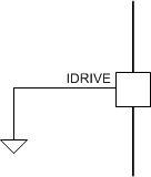 |
| 33 kΩ ± 5% to GND | 0.7 V ± 5% | High-side: 20 mA Low-side: 20 mA | High-side: 20 mA Low-side: 20 mA | High-side: 40 mA Low-side: 40 mA | High-side: 40 mA Low-side: 40 mA | 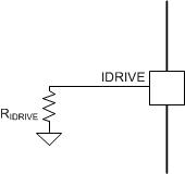 |
| 200 kΩ ± 5% to GND | 2 V ± 5% | High-side: 50 mA Low-side: 40 mA | High-side: 50 mA Low-side: 45 mA | High-side: 90 mA Low-side: 85 mA | High-side: 95 mA Low-side: 95 mA | |
| > 2 MΩ to GND, Hi-Z | 3 V ± 5% | High-side: 145 mA Low-side: 115 mA | High-side: 155 mA Low-side: 130 mA | High-side: 250 mA Low-side: 235 mA | High-side: 265 mA Low-side: 260 mA | 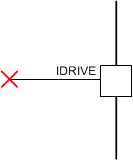 |
| 68 kΩ ± 5% to AVDD | 4 V ± 5% | High-side: 190 mA Low-side: 145 mA | High-side: 210 mA Low-side: 180 mA | High-side: 330 mA Low-side: 300 mA | High-side: 350 mA Low-side: 350 mA | 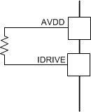 |
| < 1 kΩ to AVDD | AVDD | High-side: 240 mA Low-side: 190 mA | High-side: 260 mA Low-side: 225 mA | High-side: 420 mA Low-side: 360 mA | High-side: 440 mA Low-side:430 mA | 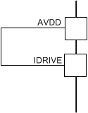 |