SLVSFL8 July 2021 DRV8770
PRODUCTION DATA
- 1 Features
- 2 Applications
- 3 Description
- 4 Revision History
- 5 Pin Configuration and Functions
- 6 Specifications
- 7 Detailed Description
- 8 Application and Implementation
- 9 Power Supply Recommendations
- 10Layout
- 11Device and Documentation Support
- 12Mechanical, Packaging, and Orderable Information
Package Options
Refer to the PDF data sheet for device specific package drawings
Mechanical Data (Package|Pins)
- RGE|24
Thermal pad, mechanical data (Package|Pins)
- RGE|24
Orderable Information
7.3.2 Pin Diagrams
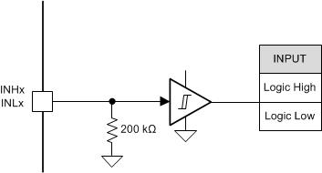
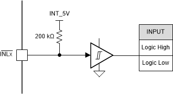
Figure 7-5 shows the input structure for the logic level pins INHx, INLx. INHx and INLx has passive pull down, so when inputs are floating the output of gate driver will be pulled low. Figure 7-6 shows the input structure for the logic level pin inverted INLx. INLx in inverted mode has passive pull up, so when inputs are floating the output of gate driver will be pulled low.
 Figure 7-5 INHx and Non-Inverted INLx Logic-Level Input
Pin Structure
 Figure 7-6 Inverted INLx Logic-Level Input Pin Structure