SLVSFL8 July 2021 DRV8770
PRODUCTION DATA
- 1 Features
- 2 Applications
- 3 Description
- 4 Revision History
- 5 Pin Configuration and Functions
- 6 Specifications
- 7 Detailed Description
- 8 Application and Implementation
- 9 Power Supply Recommendations
- 10Layout
- 11Device and Documentation Support
- 12Mechanical, Packaging, and Orderable Information
Package Options
Refer to the PDF data sheet for device specific package drawings
Mechanical Data (Package|Pins)
- RGE|24
Thermal pad, mechanical data (Package|Pins)
- RGE|24
Orderable Information
7.3.1.2 Mode (Inverting and non-inverting INLx)
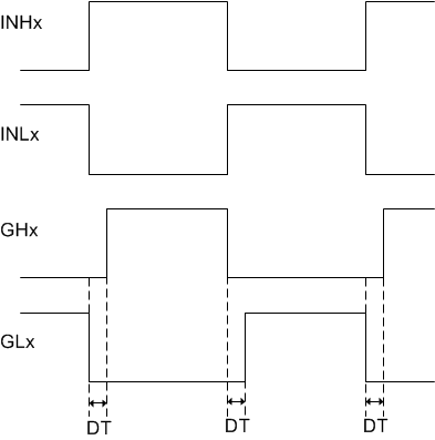
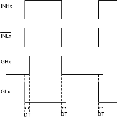
The DRV8770 has flexibility of accepting different kind of inputs on INLx. In the QFN (RGE) package variant, the MODE pin provides option of GLx output inverted or non-inverted compared to polarity of signal on INLx pin. When the MODE pin is left floating, INLx is configured to be in non-inverting mode and GLx output is in phase with INLx (see Figure 7-3). When MODE pin is connected to GVDD, GLx output is out of phase with inputs (see Figure 7-4). The TSSOP (PW) package variant does not have a MODE pin, so the INLx pins are inverted by default.
 Figure 7-3 Non-Inverted INLx inputs (MODE
= floating)
 Figure 7-4 Inverted INLx inputs (MODE =
GVDD or TSSOP package variant)
Figure 7-4 Inverted INLx inputs (MODE =
GVDD or TSSOP package variant)Table 7-1 shows the states of the gate drivers and FET half bridge when MODE = floating.
| INHx | INLx | GHx | GLx | Half Bridge State |
|---|---|---|---|---|
| 0 | 0 | L | L | Z, FETs disabled |
| 0 | 1 | L | H | L, low-side FET enabled |
| 1 | 0 | H | L | H, high-side FET enabled |
| 1 | 1 | L | L | Z, invalid state |
Table 7-2 shows the states of the gate drivers and FET half bridge for the inverted mode (MODE = GVDD or the default mode of the TSSOP package). In this mode, the INHx and INLx pins can be tied together to reduce the number of control signals from a microcontroller, as shown in Table 7-3. In this configuration, the device controls the deadtime as described in Section 7.3.1.1.2.
| INHx | INLx | GHx | GLx | Half Bridge State |
|---|---|---|---|---|
| 0 | 0 | L | H | L, low-side FET enabled |
| 0 | 1 | L | L | Z, FETs disabled |
| 1 | 0 | L | L | Z, invalid state |
| 1 | 1 | H | L | H, high-side FET enabled |
| INHx = INLx | GHx | GLx | Half Bridge State |
|---|---|---|---|
| 0 | L | H | L, low-side FET enabled |
| 1 | H | L | H, high-side FET enabled |