SLVS857B December 2009 – January 2015 DRV8808
PRODUCTION DATA.
- 1 Features
- 2 Applications
- 3 Description
- 4 Revision History
- 5 Pin Configuration and Functions
- 6 Specifications
-
7 Detailed Description
- 7.1 Overview
- 7.2 Functional Block Diagram
- 7.3
Feature Description
- 7.3.1
Setup Mode, Extended Setup Mode, Power-Down Mode
- 7.3.1.1 Operation Setup Register Bit Assignment
- 7.3.1.2 Operation Extended Setup Register Bit Assignment
- 7.3.1.3 Deep Sleep Mode
- 7.3.1.4 DC Motor Drive
- 7.3.1.5 Short/Open for Motor Outputs
- 7.3.1.6 Charge Pump
- 7.3.1.7 DC-DC Converters
- 7.3.1.8 nReset: Input for System Reset
- 7.3.1.9 VM Start-up/Power-Down and Glitch Condition
- 7.3.2 Blanking Time Insertion Timing for DC Motor Driving
- 7.3.3 Function Table in nORT, Power Down, VM Conditions
- 7.3.1
Setup Mode, Extended Setup Mode, Power-Down Mode
- 7.4 Device Functional Modes
- 7.5 Programming
- 8 Application and Implementation
- 9 Power Supply Recommendations
- 10Layout
- 11Device and Documentation Support
- 12Mechanical, Packaging, and Orderable Information
Package Options
Mechanical Data (Package|Pins)
- DCA|48
Thermal pad, mechanical data (Package|Pins)
- DCA|48
Orderable Information
1 Features
- Three DC Motor Drivers
- Up to 2.5-A Current Chopping
- Low Typical ON Resistance (RDSON = 0.5 Ω at TJ = 25°C)
- Three Integrated DC-DC Converters
- ON/OFF Selectable Using CSELECT Pin and Serial Interface
- Outputs Configurable With External Resistor Network From 1 V to 90% of VM Capability for All Three Channels
- 1.35-A Output Capability for All Three Channels
- One Integrated LDO Regulator
- Output Configurable With External Resistor Network from 1 V to 2.5 V
- 550-mA Output Capability
- 7-V to 40-V Operating Range
- Serial Interface for Communications
- Thermally Enhanced Surface-Mount Package
48-Pin HTSSOP With PowerPAD™
(Eco-Friendly: RoHS and No Sb/Br ) - Power-Down Function (Deep-Sleep Mode)
- Reset Signal Output (Active Low)
- Reset (All Clear) Control Input
2 Applications
- Printers
- Document Scanners
- POS
- Copiers
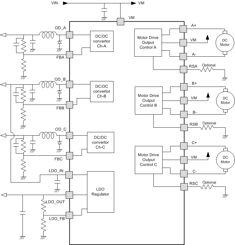
3 Description
The DRV8808 device provides the integrated motor driver solution for printers. The chip has three full H-bridges and three buck DC-DC converters.
The output driver block for each consists of N-channel power MOSFETs configured as full H-bridges to drive the motor windings. The device can be configured to use internal or external current sense for winding current control.
The SPI input pins are 3.3-V compatible and have inputs that are 5-V tolerant.
The DRV8808 has three DC-DC switched-mode buck converters to generate a programmable output voltage from 1 V up to 90% of VM, with up to 1.35-A load current capability.
The device is configured using the CSELECT terminal at start-up, and serial interface during run time.
An internal shutdown function is provided for overcurrent protection, short-circuit protection, undervoltage lockout, and thermal shutdown. Also, the device has the reset function at power on, and the input on the nReset pin.
Device Information(1)
| PART NUMBER | PACKAGE | BODY SIZE (NOM) |
|---|---|---|
| DRV8808 | HTSSOP (48) | 12.50 mm x 6.10 mm |
- For all available packages, see the orderable addendum at the end of the datasheet.
Typical Application Schematic
4 Revision History
Changes from A Revision (August 2011) to B Revision
- Added ESD Ratings table, Feature Description section, Device Functional Modes, Application and Implementation section, Power Supply Recommendations section, Layout section, Device and Documentation Support section, and Mechanical, Packaging, and Orderable Information sectionGo