SLVS857B December 2009 – January 2015 DRV8808
PRODUCTION DATA.
- 1 Features
- 2 Applications
- 3 Description
- 4 Revision History
- 5 Pin Configuration and Functions
- 6 Specifications
-
7 Detailed Description
- 7.1 Overview
- 7.2 Functional Block Diagram
- 7.3
Feature Description
- 7.3.1
Setup Mode, Extended Setup Mode, Power-Down Mode
- 7.3.1.1 Operation Setup Register Bit Assignment
- 7.3.1.2 Operation Extended Setup Register Bit Assignment
- 7.3.1.3 Deep Sleep Mode
- 7.3.1.4 DC Motor Drive
- 7.3.1.5 Short/Open for Motor Outputs
- 7.3.1.6 Charge Pump
- 7.3.1.7 DC-DC Converters
- 7.3.1.8 nReset: Input for System Reset
- 7.3.1.9 VM Start-up/Power-Down and Glitch Condition
- 7.3.2 Blanking Time Insertion Timing for DC Motor Driving
- 7.3.3 Function Table in nORT, Power Down, VM Conditions
- 7.3.1
Setup Mode, Extended Setup Mode, Power-Down Mode
- 7.4 Device Functional Modes
- 7.5 Programming
- 8 Application and Implementation
- 9 Power Supply Recommendations
- 10Layout
- 11Device and Documentation Support
- 12Mechanical, Packaging, and Orderable Information
Package Options
Mechanical Data (Package|Pins)
- DCA|48
Thermal pad, mechanical data (Package|Pins)
- DCA|48
Orderable Information
7 Detailed Description
7.1 Overview
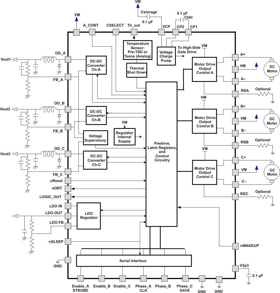
The Combo Motor Driver provides the integrated motor driver solution for printers and other applications. The chip has three full H-bridges and three Buck DC-DC converters, and one LDO.
The output driver block for each consists of N-channel power MOSFET’s configured as full H-bridges to drive the motor windings. Device can be configured to utilize internal or external current sense for winding current control.
The SPI input pins are 3.3-V compatible and 5-V tolerant inputs.
The Combo Motor Driver has three, DC-DC switch mode buck converters to generate a programmable output voltage.
The device is configured using the CSELECT terminal at start up, and serial interface during run time.
An internal shutdown function is provided for over current protection, short circuit protection, under voltage lockout and thermal shutdown.
The device also has the reset function at power on, and the input on nReset pin.
7.2 Functional Block Diagram
7.3 Feature Description
7.3.1 Setup Mode, Extended Setup Mode, Power-Down Mode
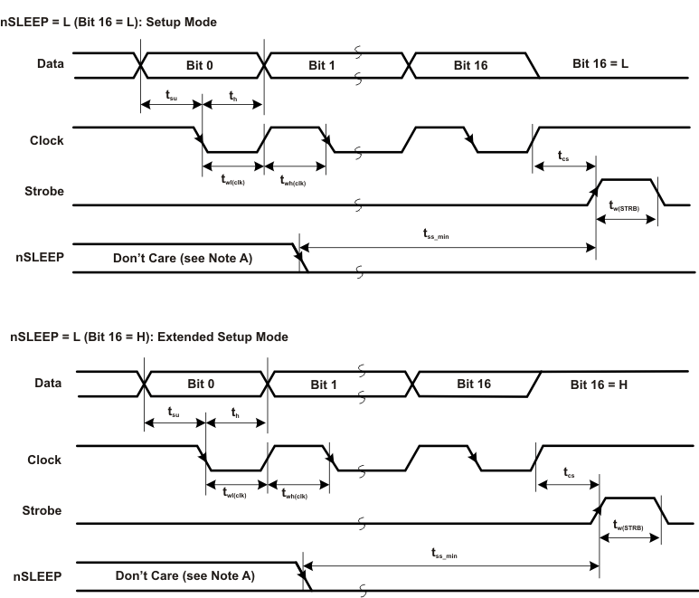
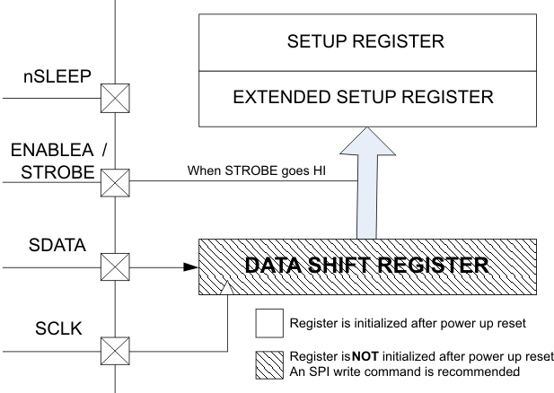
The motor output mode is configured through the SIP (DATA, CLK and STROBE) when nSLEEP = L. After set up, the nSLEEP pin must be pulled high for normal motor drive control. The value on the DATA line at the positive edge of STROBE when nSLEEP is low, selects whether the data is written to the Setup or Extended Setup registers. Setup is selected for DATA = L; Extended Setup is selected for DATA = H.
The condition, which the device requires for set up (initialize), is after the nORT (Reset) output goes H level from L level (power on, recovery from VM < 7 V). During nSLEEP in L level, all the motor-drive functions are shut down and their outputs are high-impedance state. This device forces motor-driver functions to shut down for the power-down mode, and is not damaged even if nSLEEP is asserted during motor driving.
Data is shifted at all times, regardless of nSLEEP. Care must be taken to ensure valid data has been shifted into the internal shift register, before the STROBE rising edge, occurs while nSLEEP is LO.
7.3.1.1 Operation Setup Register Bit Assignment
Table 1. Setup Registers (1)(2)(3)
| BANK | BIT | FUNCTION | DEFAULT | COMMENT |
|---|---|---|---|---|
| 0 | 0 | Tblank A 0 | 0 | 00: 3.75 μs, 01: 2.50 μs 10: 5.00 μs, 11: 6.25 μs |
| 1 | Tblank A 1 | 0 | ||
| 2 | Tblank B 0 | 0 | 00: 3.75 μs, 01: 2.50 μs 10: 5.00 μs, 11: 6.25 μs |
|
| 3 | Tblank B 1 | 0 | ||
| 4 | Tblank C 0 | 0 | 00: 3.75 μs, 01: 2.50 μs 10: 5.00 μs, 11: 6.25 μs |
|
| 5 | Tblank C 1 | 0 | ||
| 6 | DC-DC A Minoff Time | 0 | 0: 2.2 μs, 1: 6.6 μs | |
| 7 | DC-DC A SW | 1 | 0: On 1: Off |
|
| 8 | DC-DC B SW | CSELECT | ||
| 9 | DC-DC C SW | CSELECT | ||
| 10 | MOTOR CHOPPING 0 | 0 | 00: 100 kHz, 01: 50 kHz 10: 133 kHz, 11: 200 kHz |
|
| 11 | MOTOR CHOPPING 1 | 0 | ||
| 12 | RESET DELAY CONTROL | 0 | 0: Disable, 1: Enable | |
| 13 | LDO ENABLE | Note 1 | 0: On, 1: Off | |
| 14 | DC-DC B Minoff Time | 0 | 0: 2.2 μs, 1: 6.6 μs | |
| 15 | Bank Change | 0 | 0: Bank0, 1: Bank1 | |
| 1 | 0 | MISD BLANK AB 0 | 0 | 00: 2.25 μs, 01: 1.50 μs 10: 3.00 μs, 11: 3.75 μs |
| 1 | MISD BLANK AB 1 | 0 | ||
| 2 | MISD BLANK C 0 | 0 | 00: 2.25 μs, 01: 1.50 μs 10: 3.00 μs, 11: 3.75 μs |
|
| 3 | MISD BLANK C 1 | 0 | ||
| 4 | VRS A | 0 | 0: Disable, 1: Enable | |
| 5 | VRS A Level 0 | 0 | VRSA = 0: | |
| 00: 1.4 A, 01: 1.7 A 10: 1.9 A, 11: 2.2 A |
||||
| 6 | VRS A Level 1 | 0 | VRSA = 1: | |
| 00: 185 mV, 01: 210 mV 10: 260 mV, 11: 310 mV |
||||
| 7 | DC-DC C Minoff Time | 0 | 0: 2.2 μs, 1: 6.6 μs | |
| 8 | VRS B | 0 | 0: Disable, 1: Enable | |
| 9 | VRS B Level 0 | 0 | VRSB = 0: | |
| 00: 1.4 A, 01: 1.7 A 10: 1.9 A, 11: 2.2 A |
||||
| 10 | VRS B Level 1 | 0 | VRSB = 1: | |
| 00: 185 mV, 01: 210 mV 10: 260 mV, 11: 310 mV |
||||
| 11 | DEEP SLEEP | 0 | 0: Disable, 1: Enable | |
| 12 | VRS C | 0 | 0: Disable, 1: Enable | |
| 13 | VRS C Level 0 | 0 | VRSC = 0: | |
| 00: 1.4 A, 01: 1.7 A 10: 1.9 A, 11: 2.2 A |
||||
| 14 | VRS C Level 1 | 0 | VRSC = 1: | |
| 00: 185 mV, 01: 210 mV 10: 260 mV, 11: 310 mV |
||||
| 15 | Bank Change | 0 | 0: Bank0, 1: Bank1 |
7.3.1.2 Operation Extended Setup Register Bit Assignment
Table 2. Extended Setup Register (1)(2)
| BANK | BIT | FUNCTION | DEFAULT | COMMENT |
|---|---|---|---|---|
| NA | 0 | Signal Select 0 | 0 | See Logic_Out Table |
| 1 | Signal Select 1 | 0 | ||
| 2 | Signal Select 2 | 0 | ||
| 3 | Signal Select 3 | 0 | ||
| 4 | DCDC/LDO ISD Mask | 0 | 0: Disable, 1: Enable | |
| 5 | DCDC/LDO VSD Mask | 0 | 0: Disable, 1: Enable | |
| 6 | Motor ISD Mask | 0 | 0: Disable, 1: Enable | |
| 7 | TSD Mask | 0 | 0: Disable, 1: Enable | |
| 8 | Reset Mask C | 0 | 0: Disable, 1: Enable | |
| 9 | Reset Mask B | 0 | 0: Disable, 1: Enable | |
| 10 | Reset Mask A | 0 | 0: Disable, 1: Enable | |
| 11 | Reset Mask SR | 0 | 0: Disable, 1: Enable | |
| 12 | Pre TSD | 0 | 0: TSD-20C, 1: Analog output | |
| 13 | TSD Cont0 | 0 | See TSD Control Table | |
| 14 | TSD Cont1 | 0 | ||
| 15 | MISD Cont | 0 | See MISD Control Table |
Table 3. TSD Control – Operation After Detected TSD
| TSD CONT1 | TSD CONT0 | DC-DC | MOTORS | NORT | LDO | RELEASED BY |
|---|---|---|---|---|---|---|
| 0 | 0 | OFF | OFF | LOW | OFF | VM < VthVM– or nReset = L |
| 0 | 1 | ON | OFF | HIGH | ON | VM < VthVM– or nReset = L or nSLEEP L > H transition |
| 1 | 0 | ON | OFF | PULSE | ON | VM < VthVM– or nReset = L or nSLEEP L > H transition |
| 1 | 1 | OFF | OFF | LOW | OFF | VM < VthVM– or nReset = L |
Table 4. MISD Control – Operation After Detected Motor OCP
| MISD CONT | DC-DC | MOTORS | NORT | LDO | RELEASED BY |
|---|---|---|---|---|---|
| 0 | ON | OFF | PULSE (1) | ON | VM < VthVM– or nReset = L or nSLEEP L > H transition |
| 1 | OFF | OFF | LOW | OFF | VM < VthVM– or nReset = L |
Table 5. Logic_Out
| SIGNAL SELECT | FUNCTION (LOGIC_OUT OUTPUT) |
|---|---|
| 0000 | Detect OCP/UVP/OVP on A, output L |
| 0001 | Detect OCP/UVP/OVP on B, output L |
| 0010 | Detect OCP/UVP/OVP on C, output L |
| 0011 | Detect OCP on DC-DC/LDO regulator, output L |
| 0100 | Detect UVP, output L |
| 0101 | Detect OVP, output L |
| 0110 | Detect OCP on motor, output L |
| 0111 | Detect TSD, output L |
| 1000 | Revision code bit 0 |
| 1001 | Revision code bit 1 |
| 1010 | Revision code bit 2 |
| 1011 | Device code bit 0 |
| 1100 | Device code bit 1 |
| 1101 | N/A |
| 1110 | Detect OCP/UVP/OVP on LDO regulator, output L |
| 1111 | Fix, output H |
7.3.1.3 Deep Sleep Mode
Deep sleep mode can be entered by setting the deep sleep bit (bit 11) on the Setup register to HI. Once deep sleep mode is entered, every single subsystem is disabled, except the block necessary to regain power by making the nWAKEUP input pin LO.
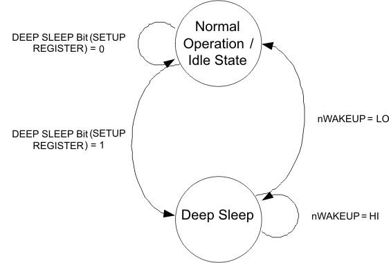 Figure 5. Deep Sleep Mode
7.3.1.4 DC Motor Drive
H-bridges A, B, and C can be controlled by using the ENABLE_X and PHASE_X control lines.
The H-bridge driver operation is available for VM > 15 V.
Internal current sense functionality is present by default. External sensing can be enabled through the serial interface. If enabled, the sense resistor must be placed externally.
NOTE
A capacitor, not larger than 2200 pF, can be placed between each H-bridge output to GND for EMI suppression purposes. It will increase the peak current but will have no impact on the operation.
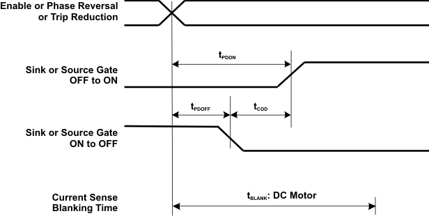 Figure 6. Crossover and Blanking Timing for H-Bridge
The dc motor H-bridges include a tBLANK period to ignore huge current spike due to rush current to varistor capacitance.
7.3.1.5 Short/Open for Motor Outputs
When a short/open situation happens, the protection circuit prevents device damage under certain conditions (short at start-up, etc).
Shutdown is released based on MISD Control in the Extended Setup register.
Table 6. DC Motor-Drive Truth Table (1)
| FAULT CONDITION | NSLEEP | ENABLEX | PHASEX | + HIGH SIDE | + LOW SIDE | – HIGH SIDE | – LOW SIDE |
|---|---|---|---|---|---|---|---|
| 0 | 0 | X | X | OFF | OFF | OFF | OFF |
| 0 | 1 | 0 | X | OFF | OFF | OFF | OFF |
| 0 | 1 | 1 | 0 | OFF | ON | ON | OFF |
| 0 | 1 | 1 | 1 | ON | OFF | OFF | ON |
| Motor OCP | X | X | X | OFF | OFF | OFF | OFF |
| TSD | X | X | X | OFF | OFF | OFF | OFF |
7.3.1.6 Charge Pump
The charge-pump voltage generator circuit utilizes, external storage, and bucket capacitors. It provides the necessary voltage to drive the high-side switches, for both DC-DC regulators and motor driver. The charge-pump circuit is driven at a frequency of 1.6 MHz (nom). Recommended bucket capacitance (connected from CP1 to CP2) is 10 nF, rated at 55 V (minimum), and storage capacitance is 0.1 μF, at 16 V (minimum). The charge-pump storage capacitor, Cstorage, should be connected from the CP output to VM.
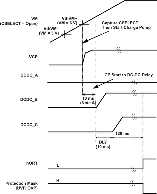
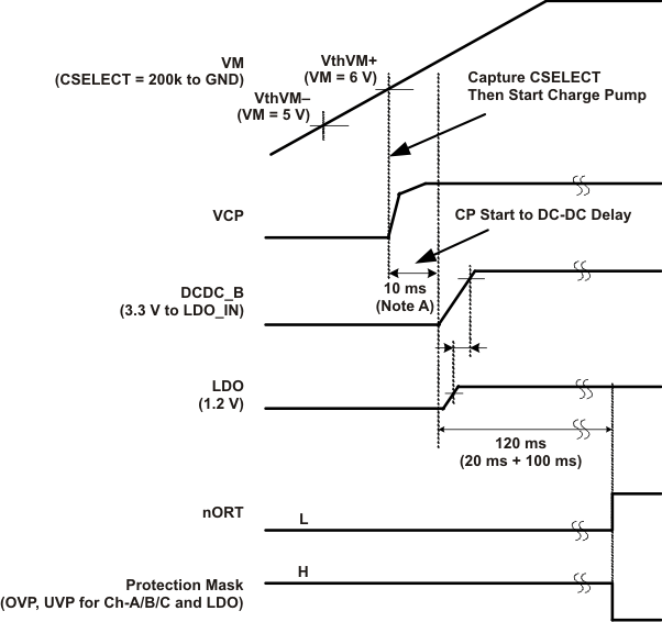
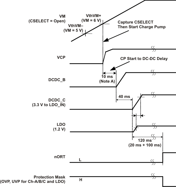
For power save in sleep mode, the charge pump is stopped when N_SLEEP = L and all three regulators are turned OFF. When the part is powered up, the charge pump is started first after the CSELECT capture and, 10 ms later from the CP startup, the first regulator is started up.
Table 7. Charge Pump (1)(2)
| FAULT CONDITION | DC-DC CH-A | DC-DC CH-B | DC-DC CH-C | NSLEEP | CHARGE PUMP |
|---|---|---|---|---|---|
| X | OFF | OFF | OFF | 0 | OFF |
| X | ON | X | X | X | ON |
| X | X | ON | X | X | ON |
| X | X | X | ON | X | ON |
| 0 | X | X | X | 1 | ON |
| Motor OCP | X | X | X | 1 | ON |
| TSD | OFF | OFF | OFF | X | OFF |
7.3.1.7 DC-DC Converters
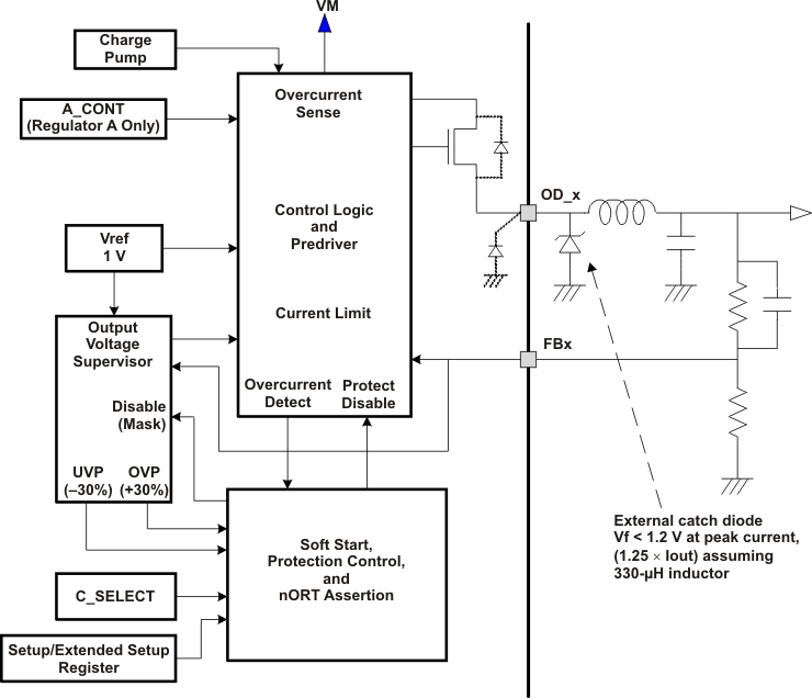 Figure 7. DC-DC Converter
This is a switch-mode regulator with integrated switches, to provide a programmed output set by the feedback terminal. The DC-DC converter has a variable duty cycle topology. External filtering (inductor and capacitor) and external catch diode are required. The output voltage is short circuit protected.
The regulator has a soft-start function to limit the rush current during start-up. It is achieved by using VFB ramp during soft start.
For unused DC-DC converter channels, the external components can be removed if the channel is set to inactive by the CSELECT pin and register bits. Recommend connecting unused FB pin to GND or V3p3 (pin 17).
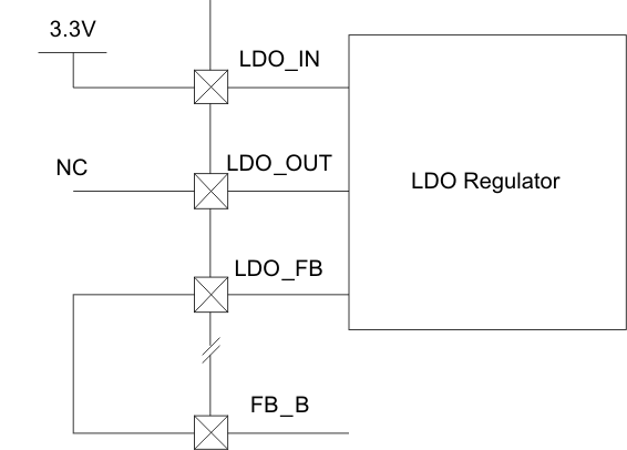 Figure 8. Unused LDO Recommended Connections
For proper termination, it is recommended that, if left unused, the LDO terminals be connected in the following fashion:
- LDO IN must be powered by an input voltage greater than 1 V.
- LDO OUT must be left disconnected.
LDO Feed Back must be connected to the DC/DC Converter Channel B Feed Back terminal.
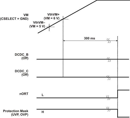
Table 8. CSELECT for Start-Up (1)(2)(3)
| CSELECT | PIN VOLTAGE | DCDC_A | DCDC_B | DCDC_C |
|---|---|---|---|---|
| Gnd | 0 V to 0.3 V | OFF | OFF | OFF |
| Pull down (by external 200 kΩ) | 1.3 V to 2.0 V | OFF | ON | OFF |
| OPEN | 3.0 V to 3.3 V | OFF | ON | ON |
Table 9. Regulator A Control
| SETUP REGISTER BANK 0, BIT 7 | A_CONT | DCDC_A |
|---|---|---|
| 0 | 0 | ON |
| 0 | 1 | OFF |
| 1 | 0 | OFF |
| 1 | 1 | OFF |
7.3.1.8 nReset: Input for System Reset
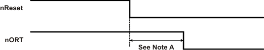
nReset pin assertion stops all the DC-DC converters and H-bridges. It also resets all the register contents to default values. After deassertion of input, device follows the initial start-up sequence. The CSELECT state is captured after the nReset deassertion (L > H).
The input is pulled up to internal 3.3 V by a 200-kΩ resistor. When the pin is H or left open, the reset function is released. Also it has deglitch filter of 2.5 μs to 7.5 μs.
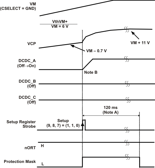
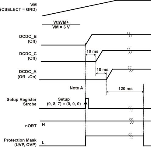
7.3.1.9 VM Start-up/Power-Down and Glitch Condition
- Start up with VM glitch (not below VthVM–)
- Start up with VM glitch (below VthVM–)
- Power down (normal)
- Power down (glitch on VM)
- Power down (glitch on VM below VthVM–)
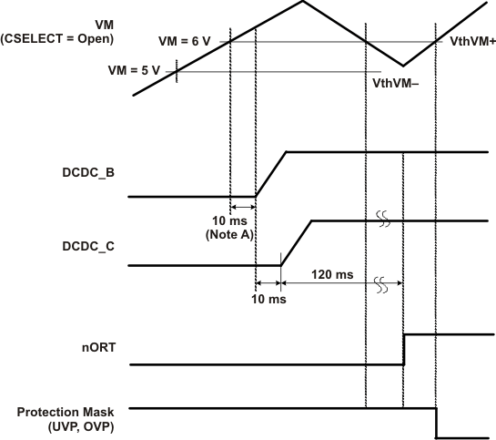
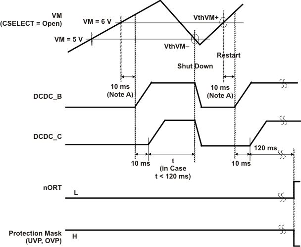
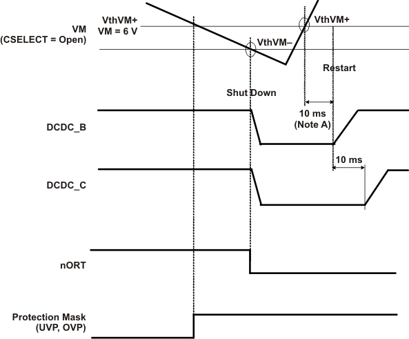
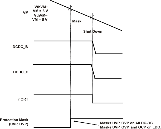 Figure 17. Power-Down Timing
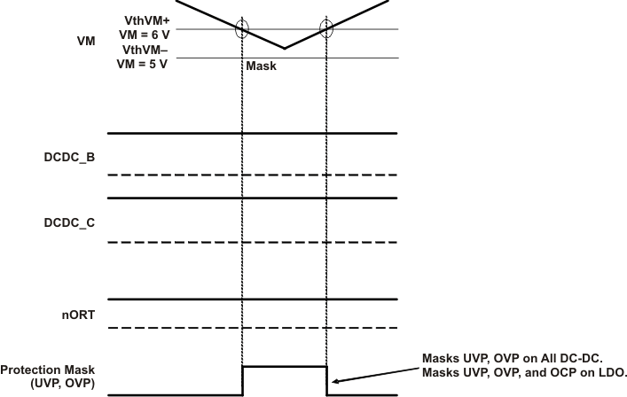 Figure 18. Power-Down Timing (With Glitch on VM)
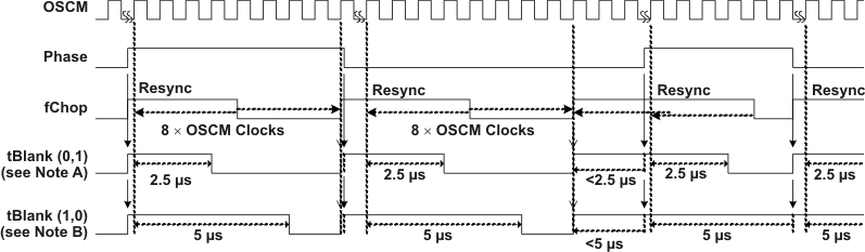
7.3.2 Blanking Time Insertion Timing for DC Motor Driving
For the dc motor-driving H-bridge, tBlank is inserted at each phase reversal and following each chopping cycle (once in every eight OSCM clocks).
For a large n number (5 or 6), tBlank setup may decrease the Itrip detect window. Care must be taken when optimizing this in the system.
Case A: Phase duty = 25%
- A*1 for setup bit = (1,0)
- A*2 for setup bit = (0,1)
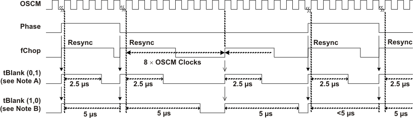
Case B: Phase duty = 40%
- B*1 for setup bit = (1,0)
- B*2 for setup bit = (0,1)
7.3.3 Function Table in nORT, Power Down, VM Conditions
The following is valid only when the protection control bits (in Extended Setup register) are all 0.
Table 10. Block Conditions by Device Status
| DEVICE STATUS | CHARGE PUMP | OSCM | nORT | MODE SETTING |
|---|---|---|---|---|
| nSleep | Active | Active | Inactive | Available |
| nORT | Inactive | Active | Active | Depend on power down |
| VM < 6 V during power down | Active | Active | See timing chart | Depend on power down |
| 4.5 V < VM | Inactive | Inactive | Active | Unavailable |
Table 11. Shutdown Functions
| FAULT CONDITION | DCDC_A | DCDC_B | DCDC_C | MOTOR | nORT |
|---|---|---|---|---|---|
| DCDC_A UVP/OVP/OCP | Shut down | Shut down | Shut down | Shut down | Asserted (low) |
| DCDC_B UVP/OVP/OCP | Shut down | Shut down | Shut down | Shut down | Asserted (low) |
| DCDC_C UVP/OVP/OCP | Shut down | Shut down | Shut down | Shut down | Asserted (low) |
| Motor OCP | See MISD Control Table | See MISD Control Table | See MISD Control Table | See MISD Control Table | See MISD Control Table |
| TSD | See TSD Control Table | See TSD Control Table | See TSD Control Table | See TSD Control Table | See TSD Control Table |
- Table is valid when the Protection and Reset Mask bits in the Extended Setup register are all 0.
- If Reset Mask (selective shutdown) bits are set, shutdown and release description is in the note following the Extended Setup register definition.
- DC-DC regulators are released at VM > VthVM+ when VM increasing. When VM decreasing, regulators are shut down when VM < VthVM–. When VthVM+ > VM > VthVM–, OVP and UVP are masked.
- Motor OCP shutdown release is specified in MISD Control Table.
- TSD shutdown release is specified in TSD Control Table.
7.4 Device Functional Modes
7.4.1 Operation With 7 V < VM < 18 V
The devices starts operating with input voltages above 6.0 V typical. Between 7 V and 18 V, DC-DC converters can operate. Enabling motors in not allowed.
7.4.2 Operation With 18 V ≤ VM ≤ 38 V
The device can operate with full function. Both DC-DC converter and Motor Drivers can be enabled.
7.5 Programming
7.5.1 Serial Interface
The device has a serial interface port (SIP) circuit block to control DC motor H-bridges, DC-DC regulators, and other functions, such as blanking time, OFF time, and so forth. Because the SIP shares its three lines with three of the motor control signals, the SIP is only available when nSLEEP is low.
Table 12. Serial Interface
| nSLEEP | PIN 9 | PIN 10 | PIN 14 | SIP FUNCTIONALITY |
|---|---|---|---|---|
| L | STB | CLK | DATA | Yes |
| H | ENA | PHA | PHC | No |
Sixteen-bit serial data is shifted least significant bit (LSB) first into the serial data input (DATA) shift register on the falling edge of the serial clock (CLK). After 16-bit data transfer, the strobe signal (Strobe) rising edge latches all the shifted data. During the data transferring, Strobe voltage level is ok with L level or H level.
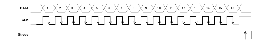 Figure 23. Serial Interface
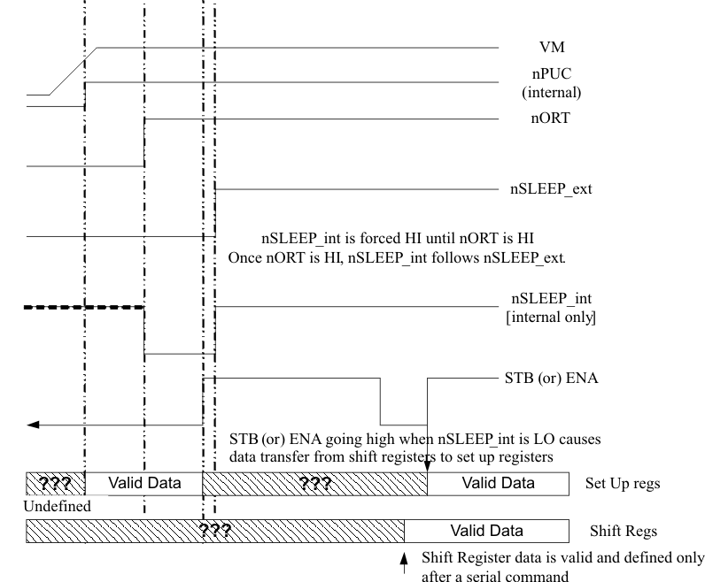
NOTE
During startup (VM rising), nSLEEP input is set HI, suppressing false data latching caused by a rising edge on the STB signal. nSLEEP will remain HI until nORT is released (120 ms after DC-DC regulators come up).