SLVS857B December 2009 – January 2015 DRV8808
PRODUCTION DATA.
- 1 Features
- 2 Applications
- 3 Description
- 4 Revision History
- 5 Pin Configuration and Functions
- 6 Specifications
-
7 Detailed Description
- 7.1 Overview
- 7.2 Functional Block Diagram
- 7.3
Feature Description
- 7.3.1
Setup Mode, Extended Setup Mode, Power-Down Mode
- 7.3.1.1 Operation Setup Register Bit Assignment
- 7.3.1.2 Operation Extended Setup Register Bit Assignment
- 7.3.1.3 Deep Sleep Mode
- 7.3.1.4 DC Motor Drive
- 7.3.1.5 Short/Open for Motor Outputs
- 7.3.1.6 Charge Pump
- 7.3.1.7 DC-DC Converters
- 7.3.1.8 nReset: Input for System Reset
- 7.3.1.9 VM Start-up/Power-Down and Glitch Condition
- 7.3.2 Blanking Time Insertion Timing for DC Motor Driving
- 7.3.3 Function Table in nORT, Power Down, VM Conditions
- 7.3.1
Setup Mode, Extended Setup Mode, Power-Down Mode
- 7.4 Device Functional Modes
- 7.5 Programming
- 8 Application and Implementation
- 9 Power Supply Recommendations
- 10Layout
- 11Device and Documentation Support
- 12Mechanical, Packaging, and Orderable Information
Package Options
Mechanical Data (Package|Pins)
- DCA|48
Thermal pad, mechanical data (Package|Pins)
- DCA|48
Orderable Information
10 Layout
10.1 Layout Guidelines
- Recommended to have GND plane layer for better thermal performance. Thermal pad directly going down to GND layer just under the device is the best way.
- Distance between Odx to Inductance should be as close as possible. This line has switching from 0 V to VM.
- FBx pin and external feedback resistor should be as close as possible. This is the analog sensing pin for the DC-DC converter.
- V3p3 pin is for internal analog reference voltage, and should be quiet. External 0.1 µF should be located closer.
10.2 Layout Example
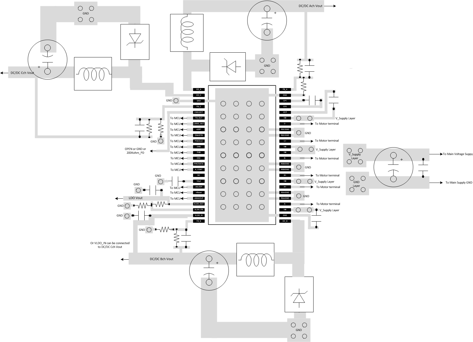 Figure 30. Layout Schematic