SLVS857B December 2009 – January 2015 DRV8808
PRODUCTION DATA.
- 1 Features
- 2 Applications
- 3 Description
- 4 Revision History
- 5 Pin Configuration and Functions
- 6 Specifications
-
7 Detailed Description
- 7.1 Overview
- 7.2 Functional Block Diagram
- 7.3
Feature Description
- 7.3.1
Setup Mode, Extended Setup Mode, Power-Down Mode
- 7.3.1.1 Operation Setup Register Bit Assignment
- 7.3.1.2 Operation Extended Setup Register Bit Assignment
- 7.3.1.3 Deep Sleep Mode
- 7.3.1.4 DC Motor Drive
- 7.3.1.5 Short/Open for Motor Outputs
- 7.3.1.6 Charge Pump
- 7.3.1.7 DC-DC Converters
- 7.3.1.8 nReset: Input for System Reset
- 7.3.1.9 VM Start-up/Power-Down and Glitch Condition
- 7.3.2 Blanking Time Insertion Timing for DC Motor Driving
- 7.3.3 Function Table in nORT, Power Down, VM Conditions
- 7.3.1
Setup Mode, Extended Setup Mode, Power-Down Mode
- 7.4 Device Functional Modes
- 7.5 Programming
- 8 Application and Implementation
- 9 Power Supply Recommendations
- 10Layout
- 11Device and Documentation Support
- 12Mechanical, Packaging, and Orderable Information
Package Options
Mechanical Data (Package|Pins)
- DCA|48
Thermal pad, mechanical data (Package|Pins)
- DCA|48
Orderable Information
5 Pin Configuration and Functions
DCA Package
48-Pins HTSSOP
Top View
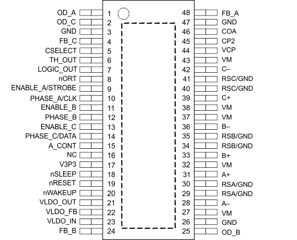
Pin Functions
| PIN | I/O | PU/PD | SHUNT R | DESCRIPTION | |
|---|---|---|---|---|---|
| NAME | NO. | ||||
| A- | 28 | O | — | — | Motor drive output for winding A- |
| A+ | 31 | O | — | — | Motor drive output for winding A+ |
| A_CONT | 15 | I | Down | 100k | DC-DC A converter control (L = Enable) |
| B- | 36 | O | — | — | Motor drive output for winding B- |
| B+ | 33 | O | — | — | Motor drive output for winding B+ |
| C- | 42 | O | — | — | Motor drive output for winding C- |
| C+ | 39 | O | — | — | Motor drive output for winding C+ |
| CP1 | 46 | O | — | — | Charge pump bucket capacitor output (low side) |
| CP2 | 45 | O | — | — | Charge pump bucket capacitor output (high side) |
| CSELECT | 5 | I | Up | 200k | DC-DC converter startup selector |
| ENA / STB | 9 | I | Down | 100k | Enable input for DC motor A control / SPI STROBE |
| ENB | 11 | I | Down | 100k | Enable input for DC motor B control |
| ENC | 13 | I | Down | 100k | Enable input for DC motor C control |
| FB_A | 48 | I | — | — | Feedback signal for DC-DC converter A |
| FB_B | 24 | I | — | — | Feedback signal for DC-DC converter B |
| FB_C | 4 | I | — | — | Feedback signal for DC-DC converter C |
| GND | 3 | — | — | — | Ground |
| GND | 26 | — | — | — | Ground |
| GND | 47 | — | — | — | Ground |
| LOGIC_OUT | 7 | O | — | — | Information monitoring output (open drain) |
| NC | 16 | NC | — | — | Do not connect |
| nORT | 8 | O | — | — | Reset output (open drain) |
| nReset | 19 | I | Up | 200k | Reset input (L: reset, H/open: normal operation) |
| nSLEEP | 18 | I | Down | 100k | Enable/disable, SPI selector |
| nWAKEUP | 20 | I | Up | 200k | Wake-up pin for DeepSleep mode (L = WAKEUP) |
| OD_A | 1 | O | — | — | Output for DC-DC switch mode regulator A |
| OD_B | 25 | O | — | — | Output for DC-DC switch mode regulator B |
| OD_C | 2 | O | — | — | Output for DC-DC switch mode regulator C |
| PHA / CLK | 10 | I | Down | 100k | Phase input for DC motor A control / SPI CLOCK |
| PHB | 12 | I | Down | 100k | Phase input for DC motor B control |
| PHC / DATA | 14 | I | Down | 100k | Phase input for DC motor C control / SPI DATA |
| RSA / GND | 30 | O | — | — | Motor drive current sensing resistor A / GND power |
| RSKA / GND | 29 | I | — | — | Motor drive current sensing resistor A / GND Kelvin |
| RSB / GND | 35 | O | — | — | Motor drive current sensing resistor B / GND power |
| RSKB / GND | 34 | I | — | — | Motor drive current sensing resistor B / GND Kelvin |
| RSC / GND | 41 | O | — | — | Motor drive current sensing resistor C / GND power |
| RSKC / GND | 40 | I | — | — | Motor drive current sensing resistor C / GND Kelvin |
| TH_OUT | 6 | O | — | — | Temperature warning output (open drain) |
| V3p3 | 17 | O | — | — | Bypass for internal 3.3-V regulator |
| VCP | 44 | O | — | — | Charge pump output |
| VLDO_FB | 22 | I | — | — | LDO voltage regulator feed back |
| VLDO_IN | 23 | I | — | — | LDO voltage regulator input |
| VLDO_OUT | 21 | O | — | — | LDO voltage regulator output |
| VM | 27 | — | — | — | Voltage supply for motors and regulators |
| VM | 32 | — | — | — | Voltage supply for motors and regulators |
| VM | 37 | — | — | — | Voltage supply for motors and regulators |
| VM | 38 | — | — | — | Voltage supply for motors and regulators |
| VM | 43 | — | — | — | Voltage supply for motors and regulators |
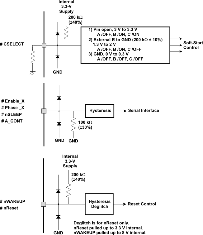 Figure 1. Input Pin Configuration
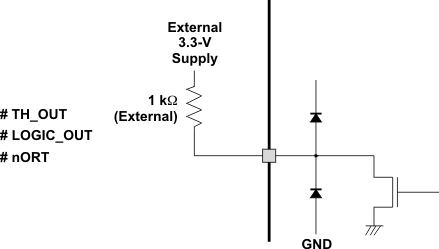 Figure 2. Open-Drain Output Pin Configuration