SLVS865J September 2008 – April 2017 DRV8811
PRODUCTION DATA.
- 1 Features
- 2 Applications
- 3 Description
- 4 Revision History
- 5 Pin Configuration and Functions
- 6 Specifications
- 7 Detailed Description
- 8 Application and Implementation
- 9 Power Supply Recommendations
- 10Layout
- 11Device and Documentation Support
- 12Mechanical, Packaging, and Orderable Information
Package Options
Mechanical Data (Package|Pins)
- PWP|28
Thermal pad, mechanical data (Package|Pins)
- PWP|28
Orderable Information
7 Detailed Description
7.1 Overview
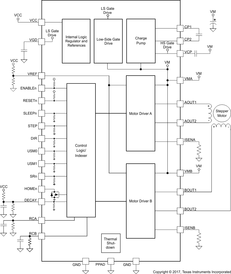
The DRV8811 device is a highly configurable, integrated motor driver solution for bipolar stepper motors. The device integrates two H-bridges, current sense and regulation circuitry, and a microstepping indexer. The DRV8811 device can be powered with a supply voltage between 8 V and 38 V and is capable of providing an output current up to 1.9 A full-scale.
A simple STEP and DIR interface allows for easy interfacing to the controller. The internal indexer is able to execute high-accuracy microstepping without requiring the controller to manage the current regulation loop.
The current regulation is highly configurable, with three decay modes of operation. They are fast, slow, and mixed decay, which can be selected depending on the application requirements. The DRV8811 device also provides configurable blanking, off time, and mixed decay, in order to adjust to a wide range of motors.
A low-power sleep mode is incorporated which allows for minimal power consumption when the system is idle.
7.2 Functional Block Diagram

7.3 Feature Description
7.3.1 PWM H-Bridge Drivers
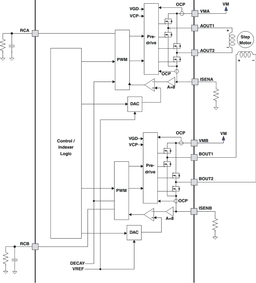
The DRV8811 device contains two H-bridge motor drivers with current-control PWM circuitry, and a microstepping indexer. A block diagram of the motor control circuitry is shown in Figure 6.
 Figure 6. Motor Control Circuitry
7.3.2 Current Regulation
The PWM chopping current is set by a comparator, which compares the voltage across a current-sense resistor, multiplied by a factor of 8, with a reference voltage. The reference voltage is input from the VREF pin. The full-scale (100%) chopping current is calculated as follows:
Example:
If a 0.22-Ω sense resistor is used and the VREF pin is 3.3 V, the full-scale (100%) chopping current is
3.3 V / (8 × 0.22 Ω) = 1.875 A.
The reference voltage is also scaled by an internal DAC that allows torque control for fractional stepping of a bipolar stepper motor, as described in the Microstepping Indexer section.
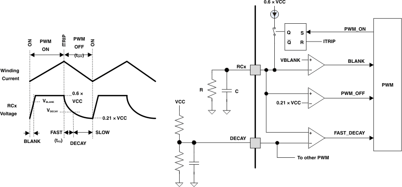
When a winding is activated, the current through it rises until it reaches the chopping current threshold described previously; then the current is switched off for a fixed off-time. The off-time is determined by the values of a resistor and capacitor connected to the RCA (for bridge A) and RCB (for bridge B) pins. The off-time is approximated by:
To avoid falsely tripping on transient currents when the winding is first activated, a blanking period is used immediately after turning on the FETs, during which the state of the current-sense comparator is ignored. The blanking time is determined by the value of the capacitor connected to the RCx pin and is approximated by:
7.3.3 Decay Mode
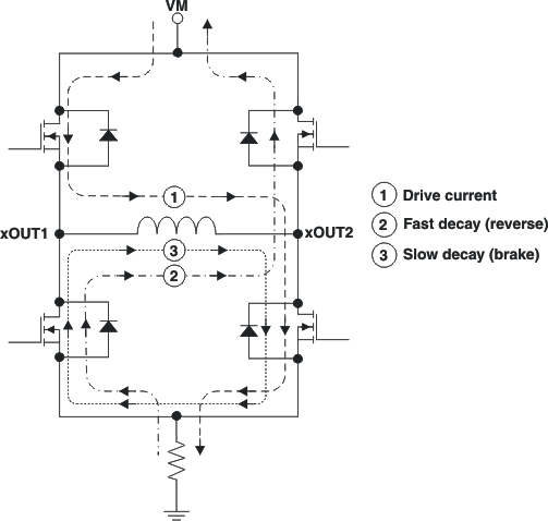
During PWM current chopping, the H-bridge is enabled to drive through the motor winding until the PWM current chopping threshold is reached. This is shown in Figure 7, Item 1. The current flow direction shown indicates positive current flow in Table 2.
Once the chopping current threshold is reached, the H-bridge can operate in two different states, fast decay or slow decay.
In fast decay mode, once the PWM chopping current level has been reached, the H-bridge reverses state to allow winding current to flow in a reverse direction. If synchronous rectification is enabled (SRn pin logic low), the opposite FETs are turned on; as the winding current approaches zero, the bridge is disabled to prevent any reverse current flow. If SRn is high, current is recirculated through the body diodes, or through external Schottky diodes. Fast-decay mode is shown in Figure 7, Item 2.
In slow-decay mode, winding current is recirculated by enabling both of the low-side FETs in the bridge. This is shown in Figure 7, Item 3.
 Figure 7. Decay Mode
The DRV8811 device also supports a mixed decay mode. Mixed decay mode begins as fast decay, but after a period of time switches to slow decay mode for the remainder of the fixed off-time.
Fast and mixed decay modes are only active if the current through the winding is decreasing; if the current is increasing, then slow decay is always used.
Which decay mode is used is selected by the voltage on the DECAY pin. If the voltage is greater than 0.6 × VCC, slow decay mode is always used. If DECAY is less than 0.21 × VCC, the device operates in fast decay mode when the current through the winding is decreasing. If the voltage is between these levels, mixed decay mode is enabled.
In mixed decay mode, the voltage on the DECAY pin sets the point in the cycle that the change to slow decay mode occurs. This time can be approximated by:
Operation of the blanking, fixed off time, and mixed decay mode is illustrated in Figure 8.
 Figure 8. PWM
7.3.4 Microstepping Indexer
Built-in indexer logic in the DRV8811 device allows a number of different stepping configurations. The USM1 and USM0 pins are used to configure the stepping format as shown in Table 1:
Table 1. Microstepping Selection Bits
| USM1 | USM0 | STEP MODE |
|---|---|---|
| 0 | 0 | Full step (2-phase excitation) |
| 0 | 1 | 1/2 step (1-2 phase excitation) |
| 1 | 0 | 1/4 step (W1-2 phase excitation) |
| 1 | 1 | 1/8 step (phase excitation) |
Table 2 shows the relative current and step directions for different settings of USM1 and USM0. At each rising edge of the STEP input, the indexer travels to the next state in the table. The direction is shown with the DIR pin high; if the DIR pin is low the sequence is reversed. Positive current is defined as xOUT1 = positive with respect to xOUT2.
Note that the home state is 45 degrees. This state is entered at power up or device reset. The HOMEn output pin is driven low in this state. In all other states it is driven logic high.
Table 2. Microstepping Indexer
| FULL STEP USM = 00 |
1/2 STEP USM = 01 |
1/4 STEP USM = 10 |
1/8 STEP USM = 11 |
AOUTx CURRENT (% FULL-SCALE) |
BOUTx CURRENT (% FULL-SCALE) |
STEP ANGLE (DEGREES) |
|---|---|---|---|---|---|---|
| 1 | 1 | 1 | 100 | 0 | 0 | |
| 2 | 98 | 20 | 11.325 | |||
| 2 | 3 | 92 | 38 | 22.5 | ||
| 4 | 83 | 56 | 33.75 | |||
| 1 | 2 | 3 | 5 | 71 | 71 | 45 (home state) |
| 6 | 56 | 83 | 56.25 | |||
| 4 | 7 | 38 | 92 | 67.5 | ||
| 8 | 20 | 98 | 78.75 | |||
| 3 | 5 | 9 | 0 | 100 | 90 | |
| 10 | –20 | 98 | 101.25 | |||
| 6 | 11 | –38 | 92 | 112.5 | ||
| 12 | –56 | 83 | 123.75 | |||
| 2 | 4 | 7 | 13 | –71 | 71 | 135 |
| 14 | –83 | 56 | 146.25 | |||
| 8 | 15 | –92 | 38 | 157.5 | ||
| 16 | –98 | 20 | 168.75 | |||
| 5 | 9 | 17 | –100 | 0 | 180 | |
| 18 | –98 | –20 | 191.25 | |||
| 10 | 19 | –92 | –38 | 202.5 | ||
| 20 | –83 | –56 | 213.75 | |||
| 3 | 6 | 11 | 21 | –71 | –71 | 225 |
| 22 | –56 | –83 | 236.25 | |||
| 12 | 23 | –38 | –92 | 247.5 | ||
| 24 | –20 | –98 | 258.75 | |||
| 7 | 13 | 25 | 0 | –100 | 270 | |
| 26 | 20 | –98 | 281.25 | |||
| 14 | 27 | 38 | –92 | 292.5 | ||
| 28 | 56 | –83 | 303.75 | |||
| 4 | 8 | 15 | 29 | 71 | –71 | 315 |
| 30 | 83 | –56 | 326.25 | |||
| 16 | 31 | 92 | –38 | 337.5 | ||
| 32 | 98 | –20 | 348.75 |
7.3.5 Protection Circuits
7.3.5.1 Overcurrent Protection (OCP)
If the current through any FET exceeds the preset overcurrent threshold, all FETs in the H-bridge are disabled until the ENABLEn pin has been brought high and then back low, or power is removed and re-applied. Overcurrent conditions are sensed in both directions; that is, any short to ground, supply, or across the motor winding results in an overcurrent shutdown.
Note that overcurrent protection does not use the current-sense circuitry used for PWM current control and is independent of the ISENSE resistor value or VVREF voltage. Additionally, in the case of an overcurrent event, the microstepping indexer is reset to the home state.
7.3.5.2 Thermal Shutdown (TSD)
If the die temperature exceeds safe limits, all drivers in the device are shut down and the indexer is reset to the home state. Once the die temperature has fallen to a safe level, operation resumes.
7.3.5.3 Undervoltage Lockout (UVLO)
If at any time the voltage on the VM pins falls below the undervoltage-lockout threshold voltage, all circuitry in the device is disabled and the indexer is reset to the home state. Operation resumes when VM rises above the UVLO threshold.
7.4 Device Functional Modes
7.4.1 RESETn, ENABLEn and SLEEPn Operation
The RESETn pin, when driven low, resets the indexer to the home position shown in Table 2. It also disables the H-bridge drivers. The STEP input is ignored while RESETn is active.
The ENABLEn pin is used to control the output drivers. When ENABLEn is low, the output H-bridges are enabled. When ENABLEn is high, the H-bridges are disabled and the outputs are in a high-impedance state.
Note that when ENABLEn is high, the input pins and control logic, including the indexer (STEP and DIR pins) are still functional.
The SLEEPn pin is used to put the device into a low-power state. If SLEEPn is low, the H-bridges are disabled, the gate drive charge pump is stopped, and all internal clocks are stopped. In this state, all inputs are ignored until the SLEEPn pin returns high.


