SLVSB19D February 2012 – March 2015 DRV8834
PRODUCTION DATA.
- 1 Features
- 2 Applications
- 3 Description
- 4 Simplified Schematic
- 5 Revision History
- 6 Pin Configuration and Functions
- 7 Specifications
- 8 Detailed Description
- 9 Application and Implementation
- 10Power Supply Recommendations
- 11Layout
- 12Device and Documentation Support
- 13Mechanical, Packaging, and Orderable Information
Package Options
Mechanical Data (Package|Pins)
Thermal pad, mechanical data (Package|Pins)
Orderable Information
8 Detailed Description
8.1 Overview
The DRV8834 supports two configurations: phase/enable mode, where the outputs are controlled by phase (direction) and enable signals for each H-bridge, and indexer mode, which allow control of a stepper motor using simple step and direction inputs.
DC motors can only be controlled in phase/enable mode; indexer mode is not applicable to DC motors.
Stepper motors can be controlled using either phase/enable load, or indexer mode.
The device is configured to be controlled either way using CONFIG pin. Logic HIGH on the CONFIG pin puts the device in the STEP/DIR mode; logic LOW lets the motor to be controlled using the xPHASE/xENBL pins.
The state of the CONFIG pin is latched at power up, and also whenever exiting sleep mode. CONFIG has an internal pulldown resistor.
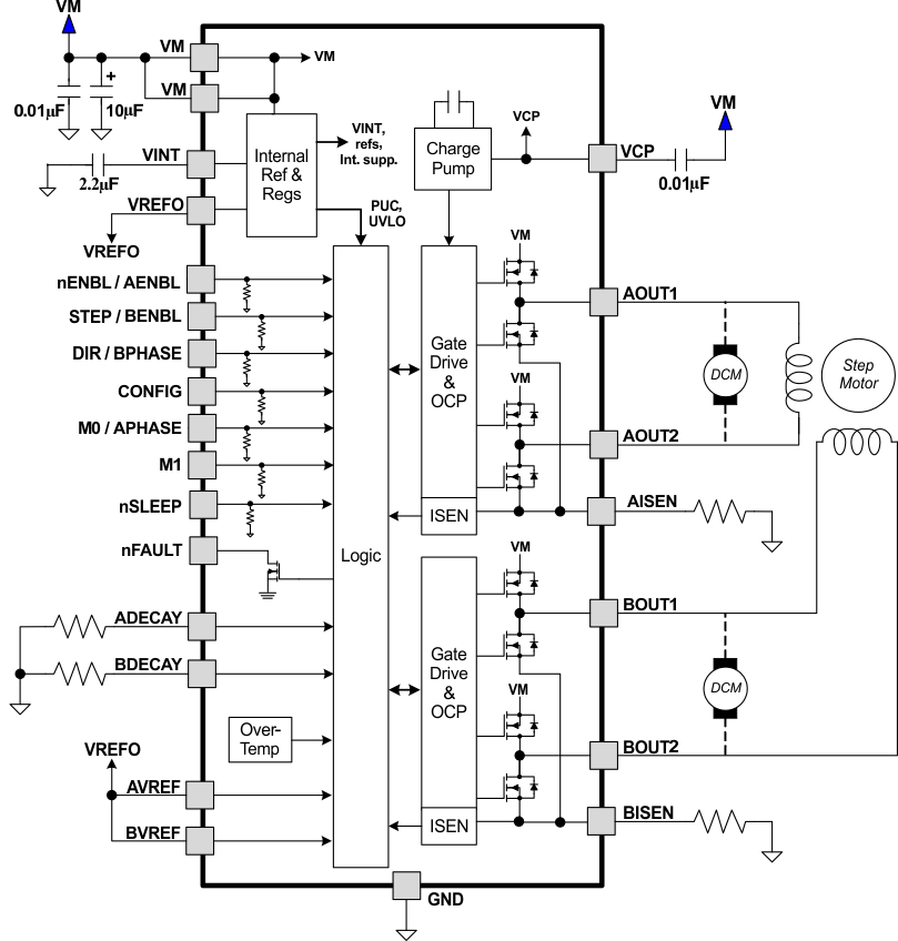
8.2 Functional Block Diagram

8.3 Feature Description
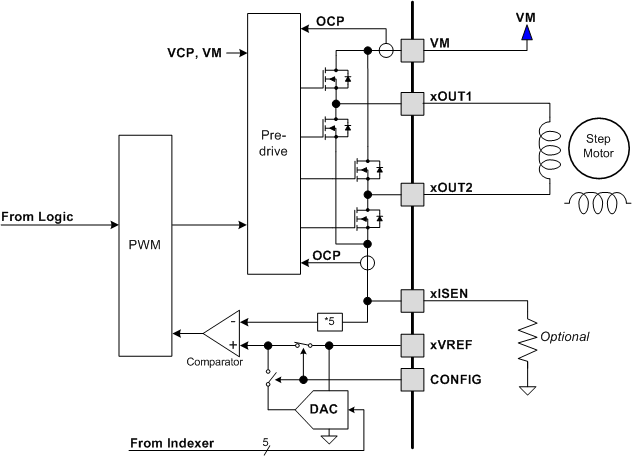
DRV8834 contains two identical H-bridge motor drivers with current-control PWM circuitry. A block diagram of the circuitry is shown in Figure 6:
 Figure 6. Motor Control Circuitry
8.3.1 Current Control
The current through the motor windings may be regulated by a fixed-frequency PWM current regulation (current chopping).
With stepping motors, current control is normally used at all times. Often it is used to vary the current in the two windings in a sinusoidal fashion to provide smooth motion. This is referred to as microstepping. The DRV8834 can provide up to 1/32 step microstepping, using internal 5-bit DACs. Finer microstepping can be implemented using the xPHASE/xENBL signals to control the stepper motor, and varying the xVREF voltages. The current flowing through the corresponding H-bridge varies according to the equation given below. A very high degree of microstepping can be achieved through this technique.
With DC motors, current control can be used to limit the start-up current of the motor to less than the stall current of the motor.
Current regulation works as follows:
When an H-bridge is enabled, current rises through the winding at a rate dependent on the supply voltage and inductance of the winding. If the current reaches the current chopping threshold, the bridge disables the current until the beginning of the next PWM cycle. Immediately after the current is enabled, the voltage on the xISEN pin is ignored for a period of time before enabling the current sense circuitry. This blanking time also sets the minimum on time of the PWM when operating in current chopping mode.
The blanking time also sets the minimum PWM duty cycle. This can cause current control errors near the zero current level when microstepping. To help eliminate this error, the DRV8834 has a dynamic tBLANK time. When the commanded current is low, the blanking period is reduced, which in turn lowers the minimum duty cycle. This provides a smoother current transition across the zero crossing region of the current waveform. The end result is smoother and quieter motor operation.
The PWM chopping current is set by a comparator which compares the voltage across a current sense resistor connected to the xISEN pins, with a reference voltage supplied to the AVREF and BVREF pins. In indexer mode, the reference voltages are scaled by internal DACs to provide scaled currents used to perform microstepping.
The chopping current is calculated as follows:

Example: If xVREF is 2 V (as it would be if xVREF is connected directly to VREFO) and a 400-mΩ sense resistor is used, the chopping current will be 2 V / 5 × 400 mΩ = 1 A.
In indexer mode, this current value is scaled by between 5% and 100% by the internal DACs, as shown in the step table in the "Microstepping Indexer" section of the data sheet.
If current control is not needed, the xISEN pins may be connected directly to ground. In this case, TI also recommends connecting AVREF and BVREF directly to VREFO.
8.3.2 Current Recirculation and Decay Modes
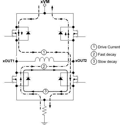
During PWM current chopping, the H-bridge is enabled to drive current through the motor winding until the PWM current chopping threshold is reached. This is shown in Figure 7 as case 1. The current flow direction shown indicates positive current flow in the step table below for indexer mode, or the current flow with xPHASE = 1 in phase/enable mode.
Once the chopping current threshold is reached, the drive current is interrupted, but due to the inductive nature of the motor, the current must continue to flow. This is called recirculation current. To handle this recirculation current, the H-bridge can operate in two different states, fast decay or slow decay.
In fast decay mode, once the PWM chopping current level has been reached, the H-bridge reverses state to allow winding current to flow in through the opposing FETs. As the winding current approaches zero, the bridge is disabled to prevent any reverse current flow. Fast decay mode is shown in Figure 7 as case 2.
In slow decay mode, winding current is recirculated by enabling both of the low-side FETs in the bridge. Slow decay is shown as case 3 in Figure 7.
 Figure 7. Decay Modes
The DRV8834 supports fast, slow, and also mixed decay modes. With DC motors, slow decay is nearly always used to minimize current ripple and optimize speed control; with stepper motors, the decay mode is chosen for a given stepper motor and operating conditions to minimize mechanical noise and vibration.
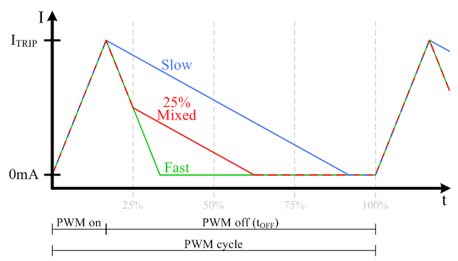
In mixed decay mode, the current recirculation begins as fast decay, but at a fixed period of time (determined by the state of the xDECAY pins shown in Table 1) switches to slow decay mode for the remainder of the fixed PWM period.
Table 1. Decay Pin Configuration
| RESISTANCE ON xDECAY PIN | -OR- VOLTAGE FORCED ON xDECAY PIN | % OF PWM CYCLE IS FAST DECAY |
|---|---|---|
| < 1 kΩ | < 0.1 V | 0% |
| 20 kΩ ±5% | 0.2 V ±5% | 25% |
| 50 kΩ ±5% | 0.5 V ±5% | 50% |
| 100 kΩ ±5% | 1 V ±5% | 75% |
| > 200 kΩ | > 2 V | 100% |
Figure 8 shows the current waveforms in slow, 25% mixed, and fast decay modes.
 Figure 8. Current Decay Modes
Decay mode is selected by the voltage present on the xDECAY pins. Internal current sources of 10 µA (typical) are connected to the pins, which allows setting of the decay mode by a resistor connected to ground if desired.
It is possible to drive the xDECAY pin with a tristate GPIO pin and also place the resistor to ground. This allows a microcontroller to select fast, slow, or mixed decay modes by driving the pin high, low, or high-impedance. The logic-low voltage must be less than 0.1 V with 10-µA of current sourced from the DRV8834 to attain slow decay.
In indexer mode, only the ADECAY pin is used, and slow decay mode is always used when at any point in the step table where the current is increasing. When current is decreasing or remaining constant, the decay mode used will be fast, slow, or mixed, as commanded by the ADECAY pin.
8.3.3 Protection Circuits
The DRV8834 is fully protected against undervoltage, overcurrent and overtemperature events.
8.3.3.1 Overcurrent Protection (OCP)
An analog current limit circuit on each FET limits the current through the FET by limiting the gate drive. If this analog current limit persists for longer than the OCP deglitch time (tOCP), all FETs in the H-bridge are disabled and the nFAULT pin are driven low. The driver will be re-enabled after the OCP retry period (approximately 1.2 ms) has passed. nFAULT becomes high again at this time. If the fault condition is still present, the cycle repeats. If the fault is no longer present, normal operation resumes and nFAULT remains deasserted. Only the H-bridge in which the OCP is detected will be disabled while the other bridge will function normally.
Overcurrent conditions are detected independently on both high-side and low-side devices; that is, a short to ground, supply, or across the motor winding will all result in an overcurrent shutdown. Overcurrent protection does not use the current sense circuitry used for PWM current control, so functions even without presence of the xISEN resistors.
8.3.3.2 Thermal Shutdown (TSD)
If the die temperature exceeds safe limits, all FETs in the H-bridge will be disabled and the nFAULT pin will be driven low. When the die temperature falls to a safe level, operation automatically resumes and nFAULT becomes inactive.
8.3.3.3 Undervoltage Lockout (UVLO)
If at any time the voltage on the VM pin falls below the undervoltage lockout threshold voltage, all circuitry in the device will be disabled, and all internal logic will be reset. Operation will resume when VM rises above the UVLO threshold. The nFAULT pin is driven low during an undervoltage condition, and also at power up or sleep mode, until the internal power supplies have stabilized.
8.4 Device Functional Modes
8.4.1 Phase/Enable Mode
In phase/enable mode, the xPHASE input pins control the direction of current flow through each H-bridge. This sets the direction of rotation of a DC motor, or the direction of the current flow in a stepper motor winding. Driving the xENBL input pins active high enables the H-bridge outputs. This can be used as PWM speed control of a DC motor, or to enable/disable the current in a stepper motor.
In phase/enable mode, the M1 input pin controls the state of the H-bridges when xENBL = 0. If M1 is high, the outputs are disabled (high impedance) when xENBL = 0; this corresponds to asynchronous fast decay mode, and is usually used in stepper motor applications to command a "zero current" state. If M1 is low, then the outputs are both driven low; this corresponds to slow decay or brake mode, and is usually used when controlling the speed of a DC motor by PWMing the xENBL pin.
Table 2. H-Bridge Control Using Phase/Enable Mode
| M1 | xENBL | xPHASE | xOUT1 | xOUT2 |
|---|---|---|---|---|
| 1 | 0 | X | Z | Z |
| 0 | 0 | X | 0 | 0 |
| X | 1 | 0 | L | H |
| X | 1 | 1 | H | L |
8.4.2 Indexer Mode
To allow a simple step and direction interface to control stepper motors, the DRV8834 contains a microstepping indexer. The indexer controls the state of the H-bridges automatically. Whenever there is a rising edge at the STEP input, the indexer moves to the next step, according to the direction set by the DIR pin.
The nENBL pin is used to disable the output stage in indexer mode. When nENBL = 1, the indexer inputs are still active and will respond to the STEP and DIR input pins; only the output stage is disabled.
The indexer logic in the DRV8834 allows a number of different stepping configurations. The M0 and M1 pins are used to configure the stepping format as shown in Table 3.
Table 3. Stepping Format
| M1 | M0 | STEP MODE |
|---|---|---|
| 0 | 0 | Full step (2-phase excitation) |
| 0 | 1 | 1/2 step (1-2 phase excitation) |
| 0 | Z | 1/4 step (W1-2 phase excitation) |
| 1 | 0 | 8 microsteps/step |
| 1 | 1 | 16 microsteps/step |
| 1 | Z | 32 microsteps/step |
The M0 pin is a tri-level input. It can be driven logic low, logic high, or high-impedance (Z).
The M0 and M1 pins can be statically configured by connecting to VINT, GND, or left open, or can be driven with standard tristate microcontroller I/O port pins. Their state is latched at each rising edge of the STEP input.
The step mode may be changed on-the-fly while the motor is moving. The indexer will advance to the next valid state for the new M0/M1 setting at the next rising edge of STEP.
The home state is 45°. This state is entered after power up, after exiting undervoltage lockout, or after exiting sleep mode. This is shown in Table 4 by cells shaded yellow.
Table 4 shows the relative current and step directions for different step mode settings. At each rising edge of the STEP input, the indexer travels to the next state in the table. The direction is shown with the DIR pin high; if the DIR pin is low the sequence is reversed. Positive current is defined as xOUT1 = positive with respect to xOUT2.
Table 4. Current and Step Directions
| 1/32 STEP | 1/16 STEP | 1/8 STEP | 1/4 STEP | 1/2 STEP | FULL STEP 70% | WINDING CURRENT A | WINDING CURRENT B | ELECTRICAL ANGLE |
|---|---|---|---|---|---|---|---|---|
| 1 | 1 | 1 | 1 | 1 | 100% | 0% | 0 | |
| 2 | 100% | 5% | 3 | |||||
| 3 | 2 | 100% | 10% | 6 | ||||
| 4 | 99% | 15% | 8 | |||||
| 5 | 3 | 2 | 98% | 20% | 11 | |||
| 6 | 97% | 24% | 14 | |||||
| 7 | 4 | 96% | 29% | 17 | ||||
| 8 | 94% | 34% | 20 | |||||
| 9 | 5 | 3 | 2 | 92% | 38% | 23 | ||
| 10 | 90% | 43% | 25 | |||||
| 11 | 6 | 88% | 47% | 28 | ||||
| 12 | 86% | 51% | 31 | |||||
| 13 | 7 | 4 | 83% | 56% | 34 | |||
| 14 | 80% | 60% | 37 | |||||
| 15 | 8 | 77% | 63% | 39 | ||||
| 16 | 74% | 67% | 42 | |||||
| 17 | 9 | 5 | 3 | 2 | 1 | 71% | 71% | 45 |
| 18 | 67% | 74% | 48 | |||||
| 19 | 10 | 63% | 77% | 51 | ||||
| 20 | 60% | 80% | 53 | |||||
| 21 | 11 | 6 | 56% | 83% | 56 | |||
| 22 | 51% | 86% | 59 | |||||
| 23 | 12 | 47% | 88% | 62 | ||||
| 24 | 43% | 90% | 65 | |||||
| 25 | 13 | 7 | 4 | 38% | 92% | 68 | ||
| 26 | 34% | 94% | 70 | |||||
| 27 | 14 | 29% | 96% | 73 | ||||
| 28 | 24% | 97% | 76 | |||||
| 29 | 15 | 8 | 20% | 98% | 79 | |||
| 30 | 15% | 99% | 82 | |||||
| 31 | 16 | 10% | 100% | 84 | ||||
| 32 | 5% | 100% | 87 | |||||
| 33 | 17 | 9 | 5 | 3 | 0% | 100% | 90 | |
| 34 | –5% | 100% | 93 | |||||
| 35 | 18 | –10% | 100% | 96 | ||||
| 36 | –15% | 99% | 98 | |||||
| 37 | 19 | 10 | –20% | 98% | 101 | |||
| 38 | –24% | 97% | 104 | |||||
| 39 | 20 | –29% | 96% | 107 | ||||
| 40 | –34% | 94% | 110 | |||||
| 41 | 21 | 11 | 6 | –38% | 92% | 113 | ||
| 42 | –43% | 90% | 115 | |||||
| 43 | 22 | –47% | 88% | 118 | ||||
| 44 | –51% | 86% | 121 | |||||
| 45 | 23 | 12 | –56% | 83% | 124 | |||
| 46 | –60% | 80% | 127 | |||||
| 47 | 24 | –63% | 77% | 129 | ||||
| 48 | –67% | 74% | 132 | |||||
| 49 | 25 | 13 | 7 | 4 | 2 | –71% | 71% | 135 |
| 50 | –74% | 67% | 138 | |||||
| 51 | 26 | –77% | 63% | 141 | ||||
| 52 | –80% | 60% | 143 | |||||
| 53 | 27 | 14 | –83% | 56% | 146 | |||
| 54 | –86% | 51% | 149 | |||||
| 55 | 28 | –88% | 47% | 152 | ||||
| 56 | –90% | 43% | 155 | |||||
| 57 | 29 | 15 | 8 | –92% | 38% | 158 | ||
| 58 | –94% | 34% | 160 | |||||
| 59 | 30 | –96% | 29% | 163 | ||||
| 60 | –97% | 24% | 166 | |||||
| 61 | 31 | 16 | –98% | 20% | 169 | |||
| 62 | –99% | 15% | 172 | |||||
| 63 | 32 | –100% | 10% | 174 | ||||
| 64 | –100% | 5% | 177 | |||||
| 65 | 33 | 17 | 9 | 5 | –100% | 0% | 180 | |
| 66 | –100% | –5% | 183 | |||||
| 67 | 34 | –100% | –10% | 186 | ||||
| 68 | –99% | –15% | 188 | |||||
| 69 | 35 | 18 | –98% | –20% | 191 | |||
| 70 | –97% | –24% | 194 | |||||
| 71 | 36 | –96% | –29% | 197 | ||||
| 72 | –94% | –34% | 200 | |||||
| 73 | 37 | 19 | 10 | –92% | –38% | 203 | ||
| 74 | –90% | –43% | 205 | |||||
| 75 | 38 | –88% | –47% | 208 | ||||
| 76 | –86% | –51% | 211 | |||||
| 77 | 39 | 20 | –83% | –56% | 214 | |||
| 78 | –80% | –60% | 217 | |||||
| 79 | 40 | –77% | –63% | 219 | ||||
| 80 | –74% | –67% | 222 | |||||
| 81 | 41 | 21 | 11 | 6 | 3 | –71% | –71% | 225 |
| 82 | –67% | –74% | 228 | |||||
| 83 | 42 | –63% | –77% | 231 | ||||
| 84 | –60% | –80% | 233 | |||||
| 85 | 43 | 22 | –56% | –83% | 236 | |||
| 86 | –51% | –86% | 239 | |||||
| 87 | 44 | –47% | –88% | 242 | ||||
| 88 | –43% | –90% | 245 | |||||
| 89 | 45 | 23 | 12 | –38% | –92% | 248 | ||
| 90 | –34% | –94% | 250 | |||||
| 91 | 46 | –29% | –96% | 253 | ||||
| 92 | –24% | –97% | 256 | |||||
| 93 | 47 | 24 | –20% | –98% | 259 | |||
| 94 | –15% | –99% | 262 | |||||
| 95 | 48 | –10% | –100% | 264 | ||||
| 96 | –5% | –100% | 267 | |||||
| 97 | 49 | 25 | 13 | 7 | 0% | –100% | 270 | |
| 98 | 5% | –100% | 273 | |||||
| 99 | 50 | 10% | –100% | 276 | ||||
| 100 | 15% | –99% | 278 | |||||
| 101 | 51 | 26 | 20% | –98% | 281 | |||
| 102 | 24% | –97% | 284 | |||||
| 103 | 52 | 29% | –96% | 287 | ||||
| 104 | 34% | –94% | 290 | |||||
| 105 | 53 | 27 | 14 | 38% | –92% | 293 | ||
| 106 | 43% | –90% | 295 | |||||
| 107 | 54 | 47% | –88% | 298 | ||||
| 108 | 51% | –86% | 301 | |||||
| 109 | 55 | 28 | 56% | –83% | 304 | |||
| 110 | 60% | –80% | 307 | |||||
| 111 | 56 | 63% | –77% | 309 | ||||
| 112 | 67% | –74% | 312 | |||||
| 113 | 57 | 29 | 15 | 8 | 4 | 71% | –71% | 315 |
| 114 | 74% | –67% | 318 | |||||
| 115 | 58 | 77% | –63% | 321 | ||||
| 116 | 80% | –60% | 323 | |||||
| 117 | 59 | 30 | 83% | –56% | 326 | |||
| 118 | 86% | –51% | 329 | |||||
| 119 | 60 | 88% | –47% | 332 | ||||
| 120 | 90% | –43% | 335 | |||||
| 121 | 61 | 31 | 16 | 92% | –38% | 338 | ||
| 122 | 94% | –34% | 340 | |||||
| 123 | 62 | 96% | –29% | 343 | ||||
| 124 | 97% | –24% | 346 | |||||
| 125 | 63 | 32 | 98% | –20% | 349 | |||
| 126 | 99% | –15% | 352 | |||||
| 127 | 64 | 100% | –10% | 354 | ||||
| 128 | 100% | –5% | 357 |
8.4.3 nSLEEP Operation
Driving nSLEEP low will put the device into a low-power sleep state. In this state, the H-bridges are disabled, the gate drive charge pump is stopped, all internal logic is reset (this returns the indexer to the home state), the VINT supply is disabled, and all internal clocks are stopped. All inputs are ignored until nSLEEP returns inactive high.
Because the VINT supply is disabled during sleep mode, it cannot be used to provide a logic high signal to the nSLEEP pin. To simplify board design, the nSLEEP can be pulled up directly to the supply (VM) if it is not actively driven. Unless VM is less than 5.75 V, a pullup resistor is required.
The nSLEEP pin is protected by a Zener diode that will clamp the pin voltage to approximately 6.5 V. The pullup resistor limits the current to the input in case VM is higher than 6.5 V. The recommended pullup resistor is 20 kΩ to 50 kΩ.
When exiting sleep mode, the nFAULT pin will be briefly driven active low as the internal power supplies turn on. nFAULT will return to inactive high once the internal power supplies (including charge pump) have stabilized. This process takes some time (up to 1 ms), before the motor driver becomes fully operational.