SLVSDA5E January   2016  – March 2020 DRV8884

PRODUCTION DATA.  

  1. Features
  2. Applications
  3. Description
    1.     Device Images
      1.      Simplified Schematic
      2.      Microstepping Current Waveform
  4. Revision History
  5. Pin Configuration and Functions
    1.     Pin Functions
  6. Specifications
    1. 6.1 Absolute Maximum Ratings
    2. 6.2 ESD Ratings
    3. 6.3 Recommended Operating Conditions
    4. 6.4 Thermal Information
    5. 6.5 Electrical Characteristics
    6. 6.6 Indexer Timing Requirements
    7. 6.7 Typical Characteristics
  7. Detailed Description
    1. 7.1 Overview
    2. 7.2 Functional Block Diagram
    3. 7.3 Feature Description
      1. 7.3.1  Stepper Motor Driver Current Ratings
        1. 7.3.1.1 Peak Current Rating
        2. 7.3.1.2 RMS Current Rating
        3. 7.3.1.3 Full-Scale Current Rating
      2. 7.3.2  PWM Motor Drivers
      3. 7.3.3  Microstepping Indexer
      4. 7.3.4  Current Regulation
      5. 7.3.5  Controlling RREF With an MCU DAC
        1. 7.3.5.1 Various Sources of Error
          1. 7.3.5.1.1 VRREF, ARREF, and RREF Error
          2. 7.3.5.1.2 VDAC Error
        2. 7.3.5.2 Application-Specific Error Calculations
      6. 7.3.6  Decay Modes
        1. 7.3.6.1 Mode 1: Slow Decay for Increasing and Decreasing Current
        2. 7.3.6.2 Mode 2: Slow Decay for Increasing Current, Mixed Decay for Decreasing Current
        3. 7.3.6.3 Mode 3: Mixed Decay for Increasing and Decreasing Current
      7. 7.3.7  Blanking Time
      8. 7.3.8  Charge Pump
      9. 7.3.9  LDO Voltage Regulator
      10. 7.3.10 Logic and Multi-Level Pin Diagrams
      11. 7.3.11 Protection Circuits
        1. 7.3.11.1 VM UVLO
        2. 7.3.11.2 VCP Undervoltage Lockout (CPUV)
        3. 7.3.11.3 Overcurrent Protection (OCP)
        4. 7.3.11.4 Thermal Shutdown (TSD)
    4. 7.4 Device Functional Modes
  8. Application and Implementation
    1. 8.1 Application Information
    2. 8.2 Typical Application
      1. 8.2.1 Design Requirements
      2. 8.2.2 Detailed Design Procedure
        1. 8.2.2.1 Stepper Motor Speed
        2. 8.2.2.2 Current Regulation
        3. 8.2.2.3 Decay Modes
      3. 8.2.3 Application Curves
  9. Power Supply Recommendations
    1. 9.1 Bulk Capacitance
  10. 10Layout
    1. 10.1 Layout Guidelines
    2. 10.2 Layout Example
  11. 11Device and Documentation Support
    1. 11.1 Documentation Support
      1. 11.1.1 Related Documentation
    2. 11.2 Receiving Notification of Documentation Updates
    3. 11.3 Community Resources
    4. 11.4 Trademarks
    5. 11.5 Electrostatic Discharge Caution
    6. 11.6 Glossary
  12. 12Mechanical, Packaging, and Orderable Information

Package Options

Mechanical Data (Package|Pins)
Thermal pad, mechanical data (Package|Pins)
Orderable Information

Charge Pump

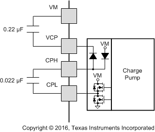
A charge pump is integrated in order to supply a high-side NMOS gate drive voltage. The charge pump requires a capacitor between the VM and VCP pins. Additionally, a low-ESR ceramic capacitor is required between pins CPH and CPL.
DRV8884 charge_pump_lvsd39.gifFigure 21. Charge Pump Diagram