SLVSD39D October   2015  – March 2020 DRV8885

PRODUCTION DATA.  

  1. Features
  2. Applications
  3. Description
    1.     Device Images
      1.      Simplified Schematic
      2.      Microstepping Current Waveform
  4. Revision History
  5. Pin Configuration and Functions
    1.     Pin Functions
  6. Specifications
    1. 6.1 Absolute Maximum Ratings
    2. 6.2 ESD Ratings
    3. 6.3 Recommended Operating Conditions
    4. 6.4 Thermal Information
    5. 6.5 Electrical Characteristics
    6. 6.6 Indexer Timing Requirements
    7. 6.7 Typical Characteristics
  7. Detailed Description
    1. 7.1 Overview
    2. 7.2 Functional Block Diagram
    3. 7.3 Feature Description
      1. 7.3.1  Stepper Motor Driver Current Ratings
        1. 7.3.1.1 Peak Current Rating
        2. 7.3.1.2 RMS Current Rating
        3. 7.3.1.3 Full-Scale Current Rating
      2. 7.3.2  PWM Motor Drivers
      3. 7.3.3  Microstepping Indexer
      4. 7.3.4  Current Regulation
      5. 7.3.5  Controlling RREF With an MCU
        1. 7.3.5.1 Various Sources of Error
          1. 7.3.5.1.1 VRREF, ARREF, and RREF Error
          2. 7.3.5.1.2 VDAC Error
        2. 7.3.5.2 Application-Specific Error Calculations
      6. 7.3.6  Decay Modes
        1. 7.3.6.1 Mode 1: Slow Decay for Increasing and Decreasing Current
        2. 7.3.6.2 Mode 2: Slow Decay for Increasing Current, Mixed Decay for Decreasing Current
        3. 7.3.6.3 Mode 3: Mixed Decay for Increasing and Decreasing Current
      7. 7.3.7  Blanking Time
      8. 7.3.8  Charge Pump
      9. 7.3.9  LDO Voltage Regulator
      10. 7.3.10 Logic and Multi-Level Pin Diagrams
      11. 7.3.11 Protection Circuits
        1. 7.3.11.1 VM Undervoltage Lockout (UVLO)
        2. 7.3.11.2 VCP Undervoltage Lockout (CPUV)
        3. 7.3.11.3 Overcurrent Protection (OCP)
        4. 7.3.11.4 Thermal Shutdown (TSD)
    4. 7.4 Device Functional Modes
  8. Application and Implementation
    1. 8.1 Application Information
    2. 8.2 Typical Application
      1. 8.2.1 Design Requirements
      2. 8.2.2 Detailed Design Procedure
        1. 8.2.2.1 Stepper Motor Speed
        2. 8.2.2.2 Current Regulation
        3. 8.2.2.3 Decay Modes
      3. 8.2.3 Application Curves
  9. Power Supply Recommendations
    1. 9.1 Bulk Capacitance
  10. 10Layout
    1. 10.1 Layout Guidelines
    2. 10.2 Layout Example
  11. 11Device and Documentation Support
    1. 11.1 Documentation Support
      1. 11.1.1 Related Documentation
    2. 11.2 Receiving Notification of Documentation Updates
    3. 11.3 Community Resources
    4. 11.4 Trademarks
    5. 11.5 Electrostatic Discharge Caution
    6. 11.6 Glossary
  12. 12Mechanical, Packaging, and Orderable Information

Package Options

Mechanical Data (Package|Pins)
Thermal pad, mechanical data (Package|Pins)
Orderable Information

Typical Characteristics

Over recommended operating conditions (unless otherwise noted)
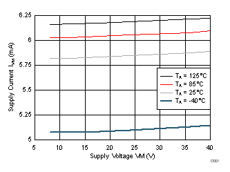
DRV8885 D001_SLVSD39.gif
Figure 2. Supply Current over VM
DRV8885 D003_SLVSD39.gif
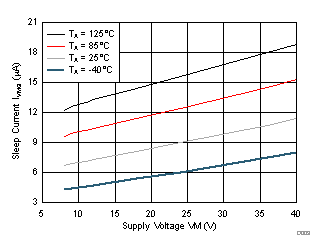
Figure 4. Sleep Current over VM
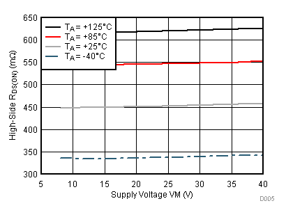
DRV8885 D005_SLVSD39.gif
Figure 6. High-Side RDS(ON) over VM
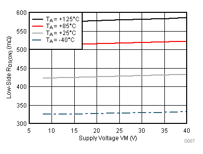
DRV8885 D007_SLVSD39.gif
Figure 8. Low-Side RDS(ON) over VM
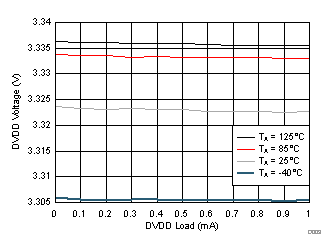
DRV8885 D009_SLVSD39.gif
Figure 10. DVDD Regulator over Load (VM = 24 V)
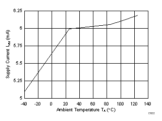
DRV8885 D002_SLVSD39.gif
Figure 3. Supply Current over Temperature (VM = 24 V)
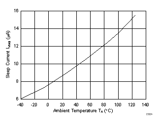
DRV8885 D004_SLVSD39.gif
Figure 5. Sleep Current over Temperature (VM = 24 V)
DRV8885 D006_SLVSD39.gif
Figure 7. High-Side RDS(ON) over Temperature (VM = 24 V)
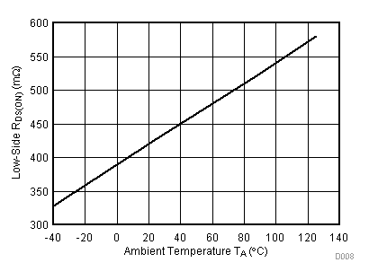
DRV8885 D008_SLVSD39.gif
Figure 9. Low-Side RDS(ON) over Temperature (VM = 24 V)
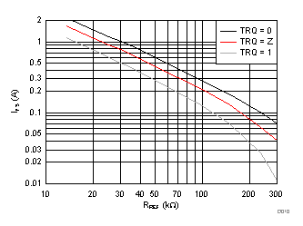
DRV8885 D010_SLVSD39.gif
Figure 11. Full-Scale Current over RREF Selection