SNLS714 September 2022 DS320PR822
PRODUCTION DATA
- 1 Features
- 2 Applications
- 3 Description
- 4 Revision History
- 5 Pin Configuration and Functions
- 6 Specifications
- 7 Detailed Description
- 8 Application and Implementation
- 9 Power Supply Recommendations
- 10Layout
- 11Device and Documentation Support
- 12Mechanical, Packaging, and Orderable Information
Package Options
Mechanical Data (Package|Pins)
- NJX|64
Thermal pad, mechanical data (Package|Pins)
Orderable Information
8.2.1.2 Detailed Design Procedure
For UPI operation, DS320PR822 is designed with linear data-path to pass the Tx Preset signaling (by CPUs) onto the Rx (of CPUs) for link training to optimize the equalization settings. The linear redriver DS320PR822 helps extend the PCB trace reach distance by boosting the attenuated signals with its equalization, which allows the user to recover the signal by the downstream Rx more easily. The DS320PR822 must be placed in between the CPU Tx and CPU Rx in such a way that signal swing at the device output pins for both Rx and Tx stays within the linearity range of the device. Adjustments to the DS320PR822 EQ setting should be performed based on the channel loss to optimize the eye opening in the Rx partner. The available EQ gain settings are provided in Table 7-1. For most systems the default flat gain setting 0 dB (GAIN = floating) would be sufficient. However, a flat gain attenuation can be utilized to apply extra equalization when needed to keep the data-path linear.
The DS320PR822 can be optimized for a given system utilizing its three configuration modes – Pin mode, SMBus/I2C Primary mode, and SMBus/I2C Secondary mode. In SMBus/I2C modes the SCL and SDA pins must be pulled up to a 3.3 V supply with a pull-up resistor. The value of the resistor depends on total bus capacitance. 4.7 kΩ is a good first approximation for a bus capacitance of 10 pF.
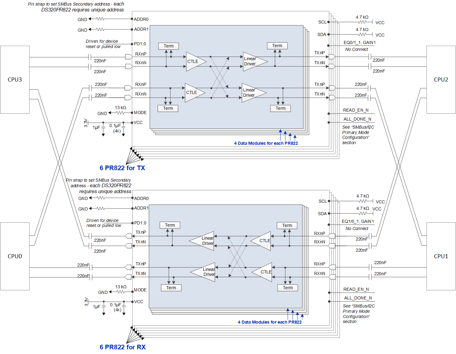
Figure 8-2 shows a simplified schematic for x24 lane configuration in SMBus/I2C Primary mode.
 Figure 8-2 Simplified Schematic for UPI x24 Lane Configuration in SMBus/I2C Primary
Mode