SNLS324F April 2011 – August 2021 DS80PCI402
PRODUCTION DATA
- 1 Features
- 2 Applications
- 3 Description
- 4 Revision History
- 5 Pin Configuration and Functions
- 6 Specifications
- 7 Parameter Measurement Information
- 8 Detailed Description
- 9 Application and Implementation
- 10Power Supply Recommendations
- 11Layout
- 12Device and Documentation Support
- 13Mechanical, Packaging, and Orderable Information
Package Options
Mechanical Data (Package|Pins)
- NJY|54
Thermal pad, mechanical data (Package|Pins)
Orderable Information
10.1 3.3-V or 2.5-V Supply Mode Operation
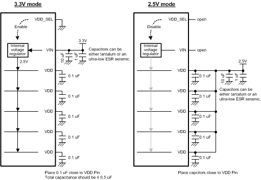
The DS80PCI402 has an optional internal voltage regulator to provide the 2.5-V supply to the device. In 3.3-V mode, the VIN pin = 3.3 V is used to supply power to the device and the VDD pins should be left open. The internal regulator will provide the 2.5 V to the VDD pins of the device and a 0.1-µF capacitor is needed at each of the five VDD pins for power supply de-coupling (total capacitance should be ≤ 0.5 µF), and the VDD pins should be left open. The VDD_SEL pin must be tied to GND to enable the internal regulator. In 2.5-V mode, the VIN pin should be left open and 2.5 V supply must be applied to the VDD pins. The VDD_SEL pin must be left open (no connect) to disable the internal regulator.
The DS80PCI402 can be configured for 2.5-V operation or 3.3-V operation. The lists below outline required connections for each supply selection.
3.3-V Mode of Operation
- Tie VDD_SEL = 0 with 1-kΩ resistor to GND.
- Feed 3.3-V supply into VIN pin. Local 1.0 µF decoupling at VIN is recommended.
- See information on VDD bypass below.
- SDA and SCL pins should connect pullup resistor to VIN
- Any 4-Level input which requires a connection to "Logic 1" should use a 1-kΩ resistor to VIN
2.5-V Mode of Operation
- VDD_SEL = Float
- VIN = Float
- Feed 2.5-V supply into VDD pins.
- See information on VDD bypass below.
- SDA and SCL pins connect pullup resistor to VDD for 2.5 V uC SMBus IO
- SDA and SCL pins connect pullup resistor to VDD for 3.3 V uC SMBus IO
- Any 4-Level input which requires a connection to "Logic 1" should use a 1-kΩ resistor to VIN
 Figure 10-1 3.3 V or 2.5 V Supply Connection Diagram