SNLS334G April 2011 – January 2015 DS80PCI800
PRODUCTION DATA.
- 1 Features
- 2 Applications
- 3 Description
- 4 Revision History
- 5 Pin Configuration and Functions
- 6 Specifications
- 7 Parameter Measurement Information
- 8 Detailed Description
- 9 Application and Implementation
- 10Power Supply Recommendations
- 11Layout
- 12Device and Documentation Support
- 13Mechanical, Packaging, and Orderable Information
Package Options
Mechanical Data (Package|Pins)
- NJY|54
Thermal pad, mechanical data (Package|Pins)
Orderable Information
1 Features
- Comprehensive Family, Proven System Interoperability
- DS80PCI102 : x1 PCIe
Gen-1, Gen-2, and Gen-3 - DS80PCI402 : x4 PCIe
Gen-1, Gen-2, and Gen-3 -
DS80PCI800 : x8/x16 PCIe
Gen-1, Gen-2, and Gen-3
- DS80PCI102 : x1 PCIe
- Automatic Rate Detect and Adaptation to Gen-1/2/3 Speeds
- Seamless Support for Gen-3 Transmit FIR Handshake
- Receiver EQ (up to 36 dB), Transmit De-Emphasis (up to 12 dB)
- Adjustable Transmit VOD: 0.8 to 1.3 Vp-p (Pin Mode)
- 0.2 UI of Residual Deterministic Jitter at 8 Gbps After 40 Inches of FR4 or 10 m 30-awg PCIe Cable
- Low Power Dissipation With Ability to Turn Off Unused Channels: 65 mW/Channel
- Automatic Receiver Detect (Hot-Plug)
- Multiple Configuration Modes: Pins/SMBus/Direct-EEPROM Load
- Flow-Thru Pinout: 54-Pin WQFN (10-mm ×
5.5-mm, 0.5-mm Pitch) - Single Supply Voltage: 2.5 or 3.3 V (Selectable)
- ±3 kV HBM ESD Rating
- −40°C to 85°C Operating Temperature Range
2 Applications
- PCI Express Gen-1, Gen-2, and Gen-3
3 Description
The DS80PCI800 is a low-power, 8-channel repeater with 4-stage input equalization, and an output de-emphasis driver to enhance the reach of PCI-Express serial links in board-to-board or cable interconnects. This device is ideal for higher density x8 and x16 PCI-Express configurations, and it automatically detects and adapts to Gen-1, Gen-2, and Gen-3 data rates for easy system upgrade.
DS80PCI800 offers programmable transmit de-emphasis (up to 12 dB), transmit VOD (up to
1300 mVp-p) and receive equalization (up to 36 dB) to enable longer distance transmission in lossy copper cables (10 meters or more), or backplanes (40 inches or more) with multiple connectors. The receiver can open an input eye that is completely closed due to inter-symbol interference (ISI) introduced by the interconnect medium.
The programmable settings can be applied easily through pins or software (SMBus/I2C), or can be loaded through an external EEPROM. When operating in the EEPROM mode, the configuration information is automatically loaded on power up, which eliminates the need for an external microprocessor or software driver.
Device Information(1)
| PART NUMBER | PACKAGE | BODY SIZE (NOM) |
|---|---|---|
| DS80PCI800 | WQFN (54) | 10.00 mm × 5.50 mm |
- For all available packages, see the orderable addendum at the end of the data sheet.
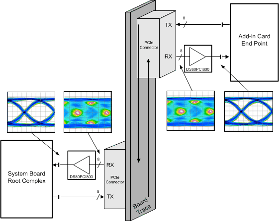
Typical Application Block Diagram
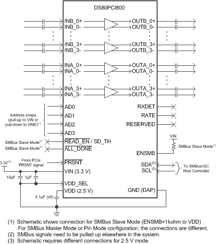
Simplified Schematic Diagram