SNLS334G April 2011 – January 2015 DS80PCI800
PRODUCTION DATA.
- 1 Features
- 2 Applications
- 3 Description
- 4 Revision History
- 5 Pin Configuration and Functions
- 6 Specifications
- 7 Parameter Measurement Information
- 8 Detailed Description
- 9 Application and Implementation
- 10Power Supply Recommendations
- 11Layout
- 12Device and Documentation Support
- 13Mechanical, Packaging, and Orderable Information
Package Options
Mechanical Data (Package|Pins)
- NJY|54
Thermal pad, mechanical data (Package|Pins)
Orderable Information
6 Specifications
6.1 Absolute Maximum Ratings(1)(2)(3)
| MIN | MAX | UNIT | |
|---|---|---|---|
| Supply voltage (VDD - 2.5-V mode) | –0.5 | 2.75 | V |
| Supply voltage (VIN - 3.3-V mode) | –0.5 | 4.0 | V |
| LVCMOS input/output voltage | –0.5 | 4.0 | V |
| CML input voltage | –0.5 | VDD + 0.5 | V |
| CML input current | –30 | 30 | mA |
| Junction temperature | 125 | °C | |
| Lead temperature soldering (4 s)(4) | 260 | °C | |
| Storage temperature, Tstg | –40 | 125 | °C |
(1) Stresses beyond those listed under Absolute Maximum Ratings may cause permanent damage to the device. These are stress ratings only, which do not imply functional operation of the device at these or any other conditions beyond those indicated under Recommended Operating Ratings. Exposure to absolute-maximum-rated conditions for extended periods may affect device reliability.
(2) Maximum Numbers are specified for a junction temperature range of –40°C to 125°C. Models are validated to Maximum Operating Voltages only.
(3) If Military/Aerospace specified devices are required, contact the Texas Instruments Sales Office/ Distributors for availability and specifications.
(4) For soldering specifications: See application note SNOA549.
6.2 ESD Ratings
| MAX | UNIT | |||
|---|---|---|---|---|
| V(ESD) | Electrostatic discharge | Human body model (HBM), per ANSI/ESDA/JEDEC JS-001, all pins(1) | ±3000 | V |
| Charged device model (CDM), per JEDEC specification JESD22-C101, all pins(2) | ±1000 | |||
| Machine model (MM), per JEDEC specification JESD22-A115-A | ±200 | |||
(1) JEDEC document JEP155 states that 500-V HBM allows safe manufacturing with a standard ESD control process.
(2) JEDEC document JEP157 states that 250-V CDM allows safe manufacturing with a standard ESD control process.
6.3 Recommended Operating Ratings
| MIN | NOM | MAX | UNIT | |
|---|---|---|---|---|
| Supply voltage (2.5-V mode) | 2.375 | 2.5 | 2.625 | V |
| Supply voltage (3.3-V mode) | 3.0 | 3.3 | 3.6 | V |
| Ambient temperature | –40 | 25 | 85 | °C |
| SMBus (SDA, SCL) | 3.6 | V | ||
| Supply noise up to 50 MHz(1) | 100 | mVp-p |
(1) Allowed supply noise (mVp-p sine wave) under typical conditions.
6.4 Electrical Characteristics
| PARAMETER | TEST CONDITIONS | MIN | TYP | MAX | UNIT | |
|---|---|---|---|---|---|---|
| POWER | ||||||
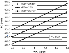
| PD | Power Dissipation | VDD = 2.5 V supply, EQ Enabled, VOD = 1.0 Vp-p, RXDET = 1, PRSNT = 0 |
500 | 700 | mW | |
| VIN = 3.3 V supply, EQ Enabled, VOD = 1.0 Vp-p, RXDET = 1, PRSNT = 0 |
660 | 900 | mW | |||
| LVCMOS / LVTTL DC SPECIFICATIONS | ||||||
| VIH25 | High-level input voltage (PRSNT, READ_EN pins) |
2.5-V Mode | 2.0 | VDD | V | |
| VIH33 | High-level input voltage (PRSNT, READ_EN pins) |
3.3-V Mode | 2.0 | VIN | V | |
| VIL | Low-Level Input Voltage (PRSNT, READ_EN pins) |
0 | 0.8 | V | ||
| VOH | High-level output voltage (ALL_DONE pin) |
IOH = −4 mA | 2.0 | V | ||
| VOL | Low-level output voltage (ALL_DONE pin) |
IOL = 4 mA | 0.4 | V | ||
| IIH | Input high current (PRSNT pin) | VIN = 3.6 V, LVCMOS = 3.6 V |
–15 | 15 | μA | |
| Input high current with internal resistors (4–level input pin) | 20 | 150 | μA | |||
| IIL | Input low current (PRSNT pin) | VIN = 3.6 V, LVCMOS = 0 V |
–15 | 15 | μA | |
| Input low current with internal resistors (4-level input pin) | –160 | –40 | μA | |||
| CML RECEIVER INPUTS (IN_n+, IN_n-) | ||||||
| RLRX-DIFF | RX differential return loss | 0.05 to 1.25 GHz | –16 | dB | ||
| 1.25 to 2.5 GHz | –16 | dB | ||||
| 2.5 to 4.0 GHz | –14 | dB | ||||
| RLRX-CM | RX common mode return loss | 0.05 to 2.5 GHz | –12 | dB | ||
| 2.5 to 4.0 GHz | –8 | dB | ||||
| ZRX-DC | RX DC single-ended impedance | Tested at VDD = 2.5 V | 40 | 50 | 60 | Ω |
| ZRX-DIFF-DC | RX DC differential mode impedance | Tested at VDD = 2.5 V | 80 | 100 | 120 | Ω |
| ZRX-HIGH-IMP-DC-POS | DC input common mode impedance for V > 0 | VID = 0 to 200 mV, ENSMB = 0, RXDET = 0, VDD = 2.5 V |
50 | kΩ | ||
| VRX-DIFF-DC | Differential RX peak-to-peak voltage (VID) | Tested at pins | 1.2 | V | ||
| VRX-SIGNAL-DET-DIFF-PP | Signal detect assert level for active data signal | SD_TH = float, 0101 pattern at 8 Gbps Measured at pins |
180 | mVp-p | ||
| VRX-IDLE-DET-DIFF-PP | Signal detect deassert level for electrical idle | SD_TH = float, 0101 pattern at 8 Gbps Measured at pins |
110 | mVp-p | ||
| HIGH-SPEED OUTPUTS | ||||||
| VTX-DIFF-PP | Output voltage differential swing | Differential measurement with OUT_n+ and OUT_n-, terminated by 50 Ω to GND, AC-Coupled, VID = 1.0 Vp-p, DEM0 = 1, DEM1 = 0(1) |
0.8 | 1.0 | 1.2 | Vp-p |
| VTX-DE-RATIO_3.5 | TX de-emphasis ratio | VOD = 1.0 Vp-p, DEM0 = 0, DEM1 = R Gen 1 & 2 modes only |
–3.5 | dB | ||
| VTX-DE-RATIO_6 | TX de-emphasis ratio | VOD = 1.0 Vp-p, DEM0 = R, DEM1 = R Gen 1 & 2 modes only |
–6 | dB | ||
| tTX-DJ | Deterministic Jitter | VID = 800 mV, PRBS15 pattern, 8.0 Gbps, VOD = 1.0 V, EQ = 0x00, DE = 0 dB (no input or output trace loss) |
0.05 | UIpp | ||
| tTX-RJ | Random Jitter | VID = 800 mV, 0101 pattern, 8.0 Gbps, VOD = 1.0 V, EQ = 0x00, DE = 0 dB, (no input or output trace loss) |
0.3 | ps RMS | ||
| tTX-RISE-FALL | TX rise/fall time | 20% to 80% of differential output voltage(3) | 35 | 45 | ps | |
| tRF-MISMATCH | TX rise/fall mismatch | 20% to 80% of differential output voltage(3) | 0.01 | 0.1 | UI | |
| RLTX-DIFF | TX differential return loss | 0.05 to 1.25 GHz | –16 | dB | ||
| 1.25 to 2.5 GHz | –12 | dB | ||||
| 2.5 to 4 GHz | –11 | dB | ||||
| RLTX-CM | TX common mode return loss | 0.05 to 2.5 GHz | –12 | dB | ||
| 2.5 to 4 GHz | –8 | dB | ||||
| ZTX-DIFF-DC | DC differential TX impedance | 100 | Ω | |||
| VTX-CM-AC-PP | TX AC peak-peak common mode voltage | VOD = 1.0 Vp-p, DEM0 = 1, DEM1 = 0(3) |
100 | mVp-p | ||
| ITX-SHORT | TX short circuit current limit | Total current the transmitter can supply when shorted to VDD or GND | 20 | mA | ||
| VTX-CM-DC-ACTIVE-IDLE-DELTA | Absolute delta of DC common mode voltage during L0 and electrical idle | (3) | 100 | mV | ||
| VTX-CM-DC-LINE-DELTA | Absolute delta of DC common mode voltgae between TX+ and TX- | (3) | 25 | mV | ||
| tTX-IDLE-DATA | Max time to transition to differential DATA signal after IDLE | VID = 1.0 Vp-p, 8 Gbps | 3.5 | ns | ||
| tTX-DATA-IDLE | Max time to transition to IDLE after differential DATA signal | VID = 1.0 Vp-p, 8 Gbps | 6.2 | ns | ||
| tPLHD/PHLD | High-to-low and low-to-high differential propagation delay | EQ = 0x00(2) | 200 | ps | ||
| tLSK | Lane-to-lane skew | T = 25°C, VDD = 2.5 V | 25 | ps | ||
| tPPSK | Part-to-part propagation delay skew | T = 25°C, VDD = 2.5 V | 40 | ps | ||
| EQUALIZATION | ||||||
| DJE1 | Residual deterministic jitter at 8 Gbps |
35” 4mils FR4, VID = 0.8 Vp-p, PRBS15, EQ = 0x1F, DEM = 0 dB |
0.14 | UIpp | ||
| DJE2 | Residual deterministic jitter at 5 Gbps |
35” 4mils FR4, VID = 0.8 Vp-p, PRBS15, EQ = 0x1F, DEM = 0 dB |
0.1 | UIpp | ||
| DJE3 | Residual deterministic jitter at 2.5 Gbps | 35” 4mils FR4, VID = 0.8 Vp-p, PRBS15, EQ = 0x1F, DEM = 0 dB |
0.05 | UIpp | ||
| DJE4 | Residual deterministic jitter at 8 Gbps |
10 meters 30-awg cable, VID = 0.8 Vp-p, PRBS15, EQ = 0x2F, DEM = 0 dB |
0.16 | UIpp | ||
| DJE5 | Residual deterministic jitter at 5 Gbps |
10 meters 30-awg cable, VID = 0.8 Vp-p, PRBS15, EQ = 0x2F, DEM = 0 dB |
0.1 | UIpp | ||
| DJE6 | Residual deterministic jitter at 2.5 Gbps | 10 meters 30-awg cable, VID = 0.8 Vp-p, PRBS15, EQ = 0x2F, DEM = 0 dB |
0.05 | UIpp | ||
| DE-EMPHASIS (GEN 1,2 MODE ONLY) | ||||||
| DJD1 | Residual deterministic jitter at 2.5 Gbps and 5.0 Gbps | 10” 4mils FR4, VID = 0.8 Vp-p, PRBS15, EQ = 0x00, VOD = 1.0 Vp-p, DEM = −3.5 dB |
0.1 | UIpp | ||
| DJD2 | Residual deterministic jitter at 2.5 Gbps and 5.0 Gbps | 20” 4mils FR4, VID = 0.8 Vp-p, PRBS15, EQ = 0x00, VOD = 1.0 Vp-p, DEM = –9 dB |
0.1 | UIpp | ||
(1) In GEN3 mode, the output VOD level is not fixed. It will be adjusted automatically based on the VID input amplitude level. The output VOD level set by DEMA/B[1:0] in GEN3 mode is dependent on the VID level and the frequency content. The DS80PCI800 repeater in GEN3 mode is designed to be transparent, so the TX-FIR (de-emphasis) is passed to the RX to support the PCIe GEN3 handshake negotiation link training.
(2) Propagation delay measurements will change slightly based on the level of EQ selected. EQ = 0x00 will result in the largest propagation delays.
(3) Parameter is characterized but not tested in production.
6.5 Electrical Characteristics — Serial Management Bus Interface
Over recommended operating supply and temperature ranges unless other specified.| PARAMETER | TEST CONDITIONS | MIN | TYP | MAX | UNIT | |
|---|---|---|---|---|---|---|
| SERIAL BUS INTERFACE DC SPECIFICATIONS | ||||||
| VIL | Data, clock input low voltage | 0.8 | V | |||
| VIH | Data, clock input high voltage | 2.1 | 3.6 | V | ||
| IPULLUP | Current through pullup resistor or current source | High Power Specification | 4 | mA | ||
| VDD | Nominal bus voltage | 2.375 | 3.6 | V | ||
| ILEAK-Bus | Input leakage per bus segment | (1) | –200 | 200 | µA | |
| ILEAK-Pin | Input leakage per device pin | –15 | µA | |||
| CI | Capacitance for SDA and SCL | (1)(2) | 10 | pF | ||
| RTERM | External termination resistance pull to VDD = 2.5 V ± 5% or 3.3 V ± 10% | Pullup VDD = 3.3 V(1)(2)(3) | 2000 | Ω | ||
| Pullup VDD = 2.5 V(1)(2)(3) | 1000 | Ω | ||||
| SERIAL BUS INTERFACE TIMING SPECIFICATIONS | ||||||
| FSMB | Bus operating frequency | ENSMB = VDD (Slave Mode) | 400 | kHz | ||
| ENSMB = FLOAT (Master Mode) | 280 | 400 | 520 | kHz | ||
| tBUF | Bus free time between stop and start condition | 1.3 | µs | |||
| tHD:STA | Hold time after (repeated) start condition. After this period, the first clock is generated. | At IPULLUP, Max | 0.6 | µs | ||
| tSU:STA | Repeated start condition setup time | 0.6 | µs | |||
| tSU:STO | Stop condition setup time | 0.6 | µs | |||
| tHD:DAT | Data hold time | 0 | ns | |||
| tSU:DAT | Data setup time | 100 | ns | |||
| tLOW | Clock low period | 1.3 | µs | |||
| tHIGH | Clock high period | (4) | 0.6 | 50 | µs | |
| tF | Clock/data fall time | (4) | 300 | ns | ||
| tR | Clock/data rise time | (4) | 300 | ns | ||
| tPOR | Time in which a device must be operational after power-on reset | (4)(5) | 500 | ms | ||
(1) Recommended value.
(2) Recommended maximum capacitance load per bus segment is 400 pF.
(3) Maximum termination voltage should be identical to the device supply voltage.
(4) Compliant to SMBus 2.0 physical layer specification. See System Management Bus (SMBus) Specification Version 2.0, section 3.1.1 SMBus common AC specifications for details.
(5) Specified by design. Parameter not tested in production.
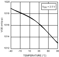
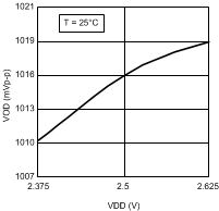
6.6 Typical Characteristics